 Fraunhofer Institute for Integrated Systems and Device Technology IISB
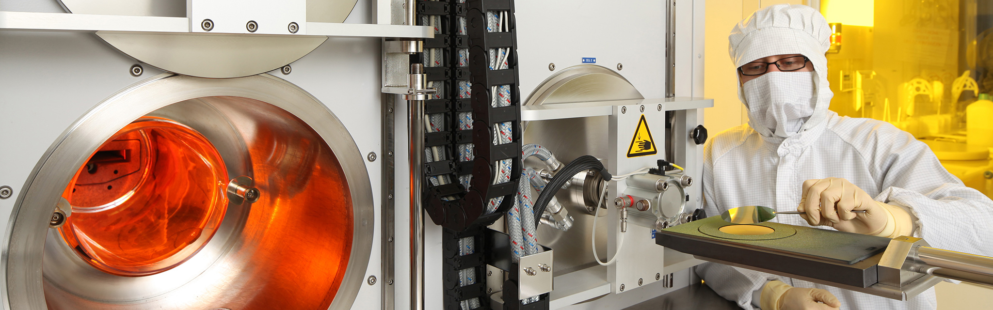
We develop the 150mm SiC epitaxy process with emphasis on improved material quality, thick epilayers, p-doping, and minority carrier lifetime. In the frame of our 200mm SiC demo lab we pioneer the epitaxy and the implant annealing on 200mm SiC substrates. State of the art metrology tools such as UV-PL or XRT together with the possibility to process complete devices in our qualified 150mm SiC line allows us to correlate the properties of the epilayer and the substrate with electrical device parameters. Based on the findings solutions are demonstrated how to overcome harmful defects.
© Kurt Fuchs / Fraunhofer IISB
Silicon Carbide
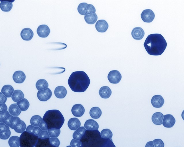
Various dislocations in SiC visualized by DSE
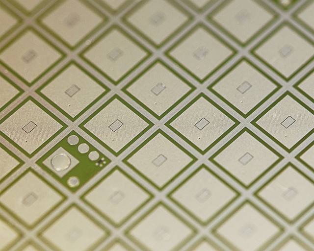
In house processed SiC power devices

Lifetime map of SiC epilayer
Services
- n- and p-type service epitaxy on 4H-SiC wafers (150mm, 200mm)
- Processing of complete SiC prototype devices (e.g. JBS, VDMOS, diodes, CMOS)
- Correlation of material defects with device performance and reliability along the whole device processing chain
- Characterization
- imaging of structural defects by x-ray topography on full wafer scale
- imaging of structural defects by combined optical surface and photoluminescence mappings on full wafer scale
- defect selective etching
- carrier lifetime measurements
- deep level transient spectroscopy (DLTS)
- mCV and FTIR measurements
- Simulation of heat and mass transport for SiC epitaxy, and other high temperature SiC specific processes
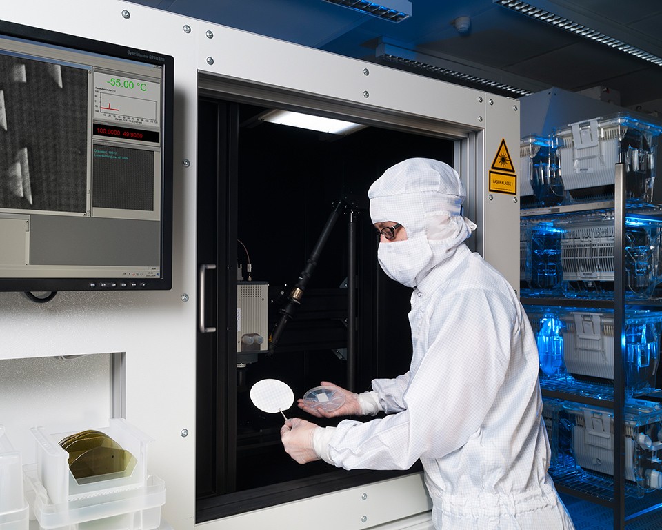
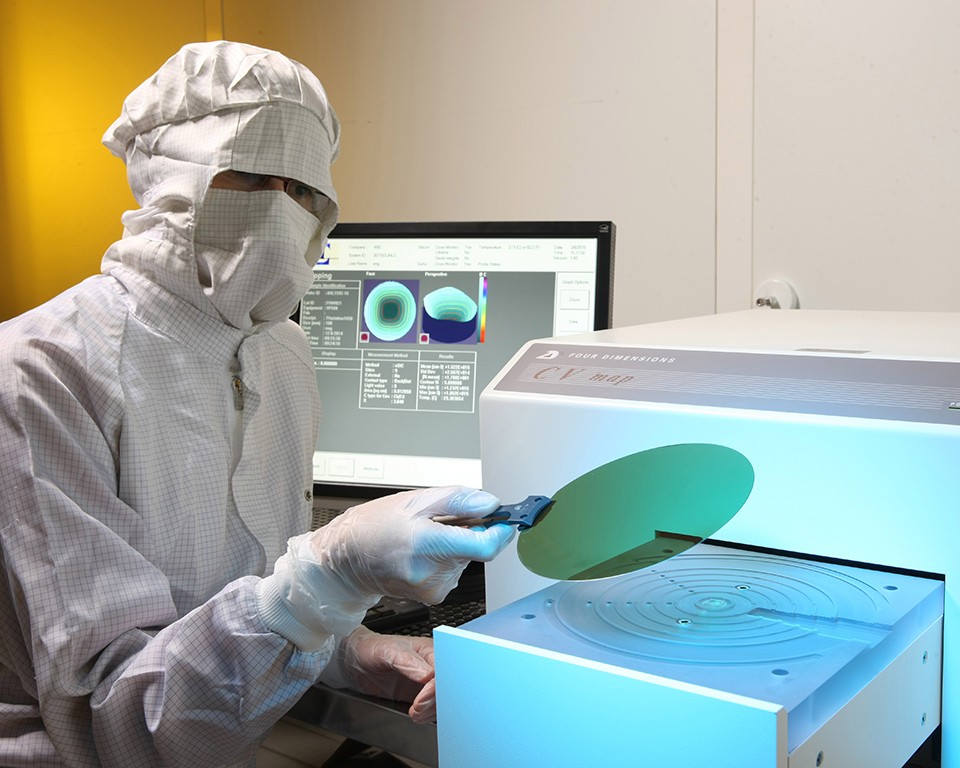
Operator loading a 100 mm SiC epiwafer in a defect luminescence scanner at Fraunhofer IISB.
Analysis of electrical properties of SiC substrates by carrier lifetime measurements and deep level transient spectroscopy (DLTS).

Full wafer scale mappings of structural defects in SiC substrates and epilayers up to 200mm diameter by x-ray topography.
TRANSFORM - European SiC Value Chain for a Greener Economy
200 mm and 150 mm SiC wafers in comparison.
With the European TRANSFORM project, the IISB is building a complete and highly competitive European supply chain for power electronics based on silicon carbide (SiC) power semiconductors.
The partners of the ECSEL project TRANSFORM, funded by the EU and the BMBF, are building a highly competitive European supply chain for SiC power electronics. One focus is the development of a semiconductor technology for future SiC substrates with 200 mm diameter, which will significantly reduce the cost of SiC power devices, as currently substrates with a diameter of 150 mm are state of the art.
In the Joint Lab in close partnership with the equipment manufacturers, the IISB is developing
- processes for an advanced multi-wafer SiC epitaxy reactor from the company Aixtron,
- novel equipment for implant activation and substrate oxidation from the company Centrotherm,
- as well as innovative material characterisation by means of X-ray topography with the company Rigaku.
The close scientific exchange also provides valuable feedback to the substrate and device manufacturers involved in the project to accelerate the transition to 200 mm technologies and to further improve quality and reliability of the substrates, epitaxial layers and devices.
TRANSFORM homepage