Lock-in Thermography

Description of lock-in thermography analysis

  • Detecting of failed power electronic devices such as IGBT, MosFETs, diodes, and resistors
  • Analysis of short circuits, ESD defects, oxide damages, edge termination defects, avalanche brake down, whiskers, and electrical conductive contamination
  • High sensitivity for hot spot detection with a heat dissipation in the μW range
  • 2D / 3D defect localization for further destructive analysis to identify the failure mechanism

Special features

  • Measurement voltage from mV up to 10kV
  • Decapsulation of mold compounds as well as silicone gels
  • Chemical removal of chip topside metallization and contacts for instance bond wires and ribbons out of different materials
  • Follow up investigations such as cross sections, scanning electron microscopy, micro sections with focused ion beam
  • Interpretation of test results and failure mechanisms
  • Consultancy on the different investigated failure modes for instance chip damage due to improper bond wire process parameters

Principles of analysis

  • The device under test is pulsed with the rectangular voltage by arbitrary Lock-In frequency (typical: 1 to 25Hz)
  • Electrical defect dissipate thermal power
  • Thermal power heats up the surface
  • Measurement of IR signal infrared camera
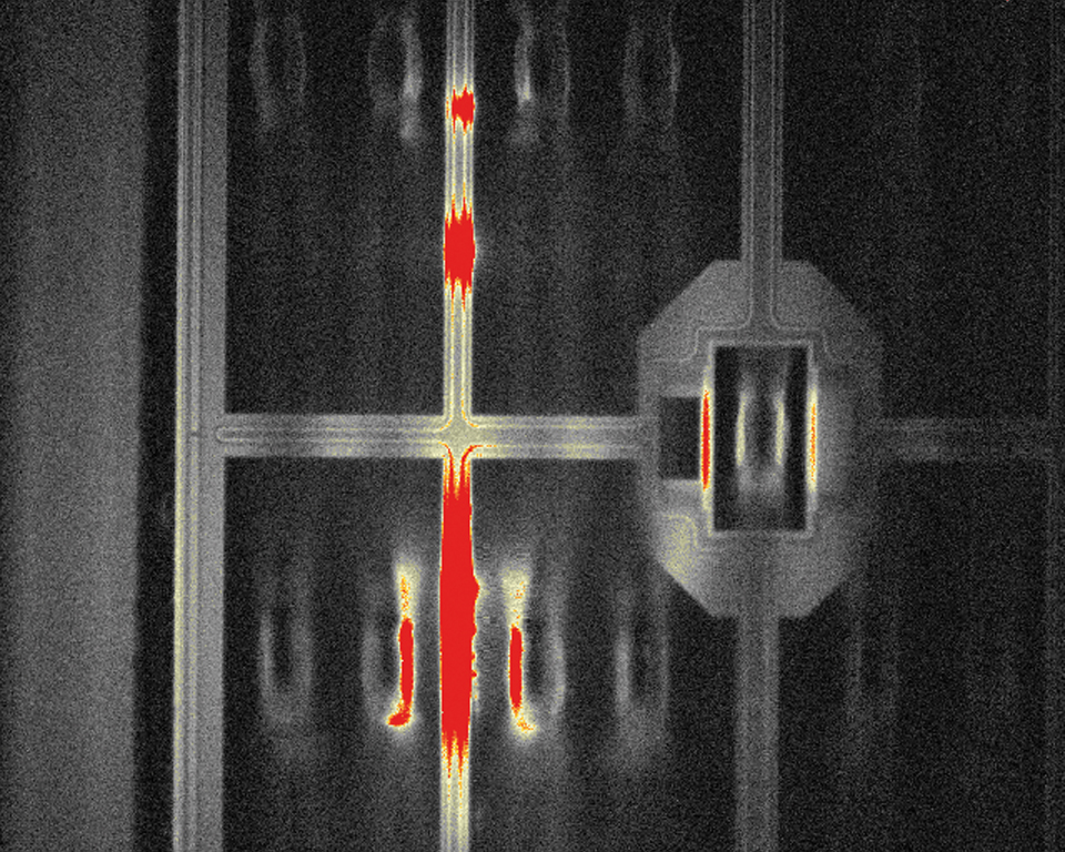
  • Acquisition of amplitude image as well as resulting time dependent step response (phase image)

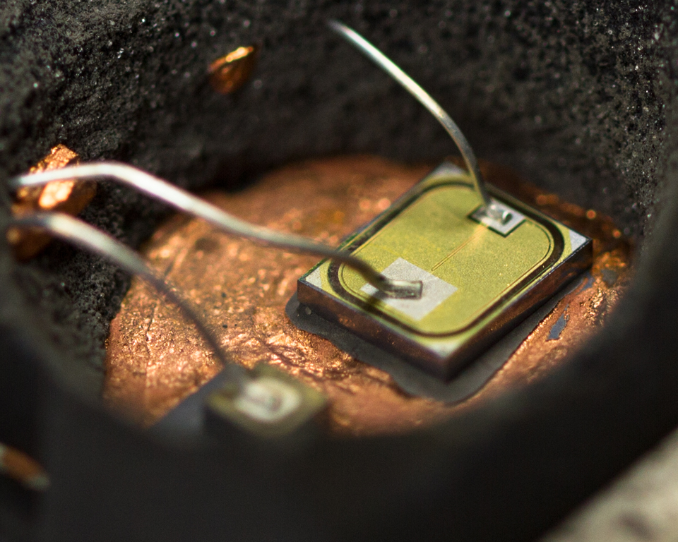
Demolded device
© Fraunhofer IISB
Demolded device
improper bond wire process parameters
© Fraunhofer IISB
improper bond wire process parameters
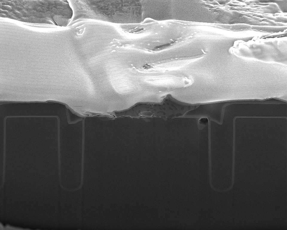
Focused ion beam analysis of an IGBTCross section
© Fraunhofer IISB
Focused ion beam analysis of an IGBT

Advantages

  • Differential measurement principle
  • Best suited for different emission coefficients of the device surface materials
  • No influence of the ambient (temperature, reflections)
  • Three different zoom lenses to investigate structures from complete power module to single IGBT cells

Application example


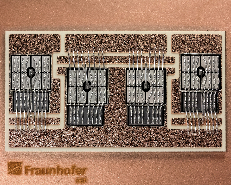
  • After fabrication, a power module failed the final electrical quality test (e.g. gate-emitter leakage current)
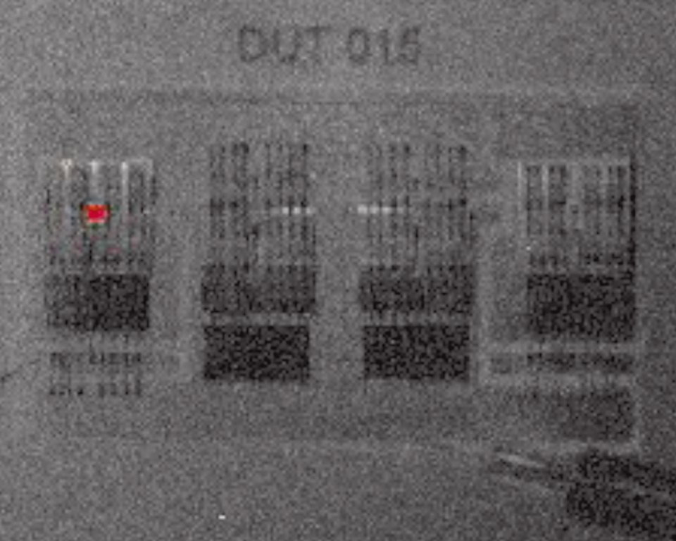
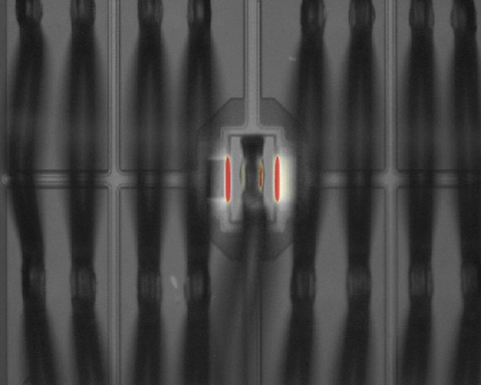
  • Lock-in thermography helps to detect which semiconductor is responsible for the leakage current and determines the exact position of the defect on the device
  • Next step consists of removing bond wires of the semi conductor followed by a second lock-in thermography analysis to get the micro scale location of the defect
  • Last step can be a focused ion beam investigation with scanning electron microscopy to detect the cause of failure (e.g. damaged gate structure)


Power modul
© Fraunhofer IISB
Power modul
Lock-in overview
© Fraunhofer IISB
Lock-in overview
Lock-in detail
© Fraunhofer IISB
Lock-in detail
 

Lock-In Thermography

[ PDF  0.57 MB ]