Packaging for Electronics

Ceramic Embedding

Using the various advantages for Wide Band Gap semiconductor devices, we investigate concepts that exhibit planar contacts, low parasitic inductance, high voltage, high design flexibility, environmental compatibility and high temperature suitability.


Download Product Sheets and Articles as PDF:

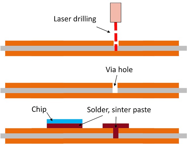
Motivation for Ceramic Embedding:

  • Miniaturization & no housing, 3D-integration, reduction of connection points
  • High switching & short current paths, vias instead of bond wires, low parasitic inductance
  • More efficient cooling & double-sided cooling, thermal vias
  • High temperature capability (> 200 °C)
  • High thermal conductivity (Al2O3, AlN, Si3N4)
  • High current carrying capability (Cu layer > 300 µm), no wires
  • High corrosion resistance (ceramic)
  • Low CTE-Mismatch

Ultra Short Pulse Laser Structuring

  • Easy DBC designing on demand
  • Cost effective and fast prototyping
  • Super fine lining
  • Electrical field control
  • Limitless trench layout for insulation
  • 3D structuring of organic, inorganic and metallic materials
  • Reverse engineering

Wire Bonding

Using new materials for bond wires like copper, composites, or alloys, we aim for improvement of the application’s lifetime. Furthermore, by bonding parameters, geometry, material, and others, we cover every power electronics application. For best bondability, we also benefit from using metallization and surface optimization of semiconductors.


    Wedge-Wedge

    Ball-Wedge

    Wire bond materials: aluminium, copper, aluminium composites, gold


Download Product Sheet as PDF:

Research fields 

  • New materials for bond wires like copper, composites, or alloys
  • Improvement of application’s lifetime by bonding parameters, geometry, material, and others
  • Metalization and surface optimization of semiconductors for best bondability
  • Cleaning process to achieve a reliable bond connection
  • In combination with power cycling tests a correlation between bonding parameters to lifetime is possible
  • Aluminum and copper wedge-wedge-bonding with diameters from 100μm to 500μm possible
  • Ribbon bonding
  • Gold ball-wedge bonding with diameters from 25μm to 75μm possible
  • Heatable work holder for bond process under temperature for up to 200°C
  • Quality assurance through pull and shear tests
  • Control of reliability and lifetime by active power cycling test, passive temperature cycling and vibration tests
  • Design of experiments to find best suited bonding parameters

Add-on: Vias in DBC Substrates for embedded power modules

Novel Via manufacturing approaches

  • Laser drilling, stencil printing, dispensing, mechanical contacting
  • Copper paste, copper rivets, silver paste

© Fraunhofer IISB

Die Bonding

Our portfolio of services contains all standard soldering techniques for chip attachments, as well as pressureless and pressure assisted sintering and next-generation silver direct bonding techniques for 3D power integration.


Silver direct bonding is an innovative die-attach technique for 3D power integration. This technology allows micro-structured devices with thin metal films to be joined together without an intermediate layer. Normally, the direct bond is formed completely under solid-state conditions without liquid phase. In case of silver finish, direct bonds exhibiting high bonding strength and good interlayer electrical conduction can be already obtained at low temperature and pressure.


TOP SIDE LEADFRAME

  • Lifetime 17x
  • Metallization of off the shelf devices
  • Ag-Sintering, top and bottom chip contact
  • Pressure assisted process
  • Pressure less process
  • Stress relieving measures
 

Download product Sheets and Articles as PDF:

Silver sintering

  • Pressureless and pressure assisted (up to 75kN) process for small and large areas
  • Single and double sided semiconductor devices
  • Multichip power modules using pre attaching
  • Selective sintering on populated circuit boards
  • Sintering of active and passive components
  • Sintering on DCB, PCB, and leadframe
  • Screening of different sinter material

Soldering

  • Standard lead free tin based and high temperature alloys
  • Void free soldering with paste and preform material

Direct Bonding

Summary:

  • No intermediate layer
  • Reduced assembly process steps
  • Reduced process costs
  • Fine pitch
  • Very high bonding strength made for power electronics

Prototypes


Full SiC Double Sided Busbar Module
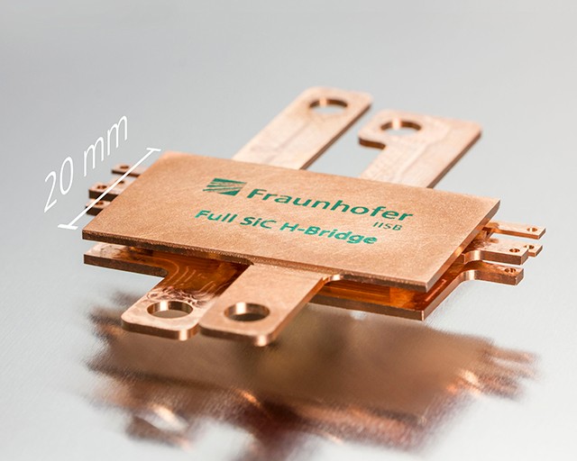
© Fraunhofer IISB

Idea of concept

  • Low inductance and high temperature power module for e-drives
  • Fast switching with SiC
  • DC+ & DC- on outer metalliztion for lowest parasitic C to ground
  • High reliability and temperature capability by silver sintering
  • Low cost due to copper busbars with hybrid polymer isulation layers instead of DBC substrates
  • Double sided cooling, high thermal capability

Further examples of our prototypes

© Fraunhofer IISB
Head spreading and CTE matching by graphite
© Fraunhofer IISB
Double sided cooled sintered power module
© Fraunhofer IISB
Double sided silver sintering of power semiconductors

Equipment & Laboratories

We operate our own clean room according to ISO classification 7 and futher laboratories for analysis and lifetime testing.

Due to our membership in the Research Fab Microelectronics Germany (FMD), we operate an advanced packaging line for power electronics, as well as an environmental laboratory for power electronics - components and systems.


Stencil printer and Ink-jet printer for sinter and solder pastes as well as printing polymers and thermal interface materials in the packaging clean room

Equipment

  • Multi-physics simulation tools (electro-thermo-mechanical), CAD
  • Plasma cleaning
  • Printer for paste material
  • Vapor-phase vacuum soldering
  • Formic-acid-activated IR vacuum reflow
  • Hydrogen activated IR vacuum reflow
  • Full automatic die placer with high temperature and extended tool force capability
  • Automatic wire and ribbon bonders (Al, Cu, Au)
  • Servo press for sintering
  • Ultrasonic and resistance welding machines for electric terminals