SiC Services

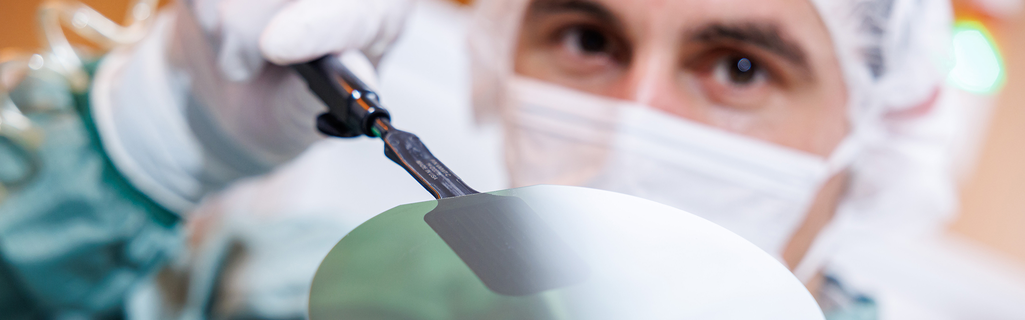
Custom-tailored SiC Services with One-stop Solutions from Material to System

Drawing on 20 years of cooperation with partners from SiC industry and research, Fraunhofer IISB has been established as Germany‘s hotspot for silicon carbide power device manufacturing on a 150 mm SiC line. Our mission is to share our many years of experience with the customers and to provide them with distinct SiC power device prototypes for newly arising markets.  We are currently ramping up our 200 mm SiC line - many tools and processes are ready and technological gaps will be closed soon.

4H-SiC is the ideal semiconductor for the realization of high-voltage and high-power electronic devices due to its outstanding material properties. With SiC services as a crosscut topic of the departments of Fraunhofer IISB and in close collaboration with the in-house brand π-Fab, we offer R&D services ranging from material development and prototype devices to module assembly and mechatronic systems.

Core competences

  • Simulation and modeling
  • Homoepitaxy and defect engineering
  • Device and circuit design
  • Full power device manufacturing
  • Wafer thinning and packaging
  • Device characterization

SiC power device prototypes

  • Diodes (SBD, PIN, MPS)
  • MOSFETs (planar, trench)
  • Specific devices (bipolar, CMOS, sensor)
  • Industry collaboration towards qualified high-volume foundries

Markets

  • Hybrid electric vehicles and electric vehicles
  • Renewable energies (wind, solar)
  • Power grid

SiC Materials

Development and optimization of SiC epitaxy processes


We develop SiC epitaxy processes with emphasis on improved material quality. State of the art metrology tools such as UV-PL or XRT together with the possibility to process complete devices allows us to correlate the properties of the epilayer and the substrate with electrical device parameters. Based on the findings, solutions are developed that allow one to overcome harmful defects. Process development is supported by the simulation of fluid dynamics, heat transfer, species transport, and chemical reactions with tailored CFD software.

In addition, the potential of SiC and diamond for quantum applications is explored. In particular, we investigate how color centers in SiC and diamond can be generated.

SiC Devices

Our SiC device activities provide one-stop solutions for development and prototype fabrication of SiC devices, circuits and systems. IISB is operating a complete 150 mm SiC process line for implementation of its prototype fabrication technologies. We offer a broad range of device-related services including proof-of-concept for new device concepts, technology development for device improvements, and small-volume fabrication for small and medium-sized enterprises. Continuous progress in TCAD process and device modeling augments the device development and helps to reduce time-to-market for our partners.

© Kurt Fuchs / Fraunhofer IISB

SiC Device Fabrication at Fraunhofer IISB

In the video, gain an insight into how the entire value chain from materials to power electronic systems is covered by the research and development activities of Fraunhofer IISB. Our 150 mm SiC pilot process line, which is unique in Europe, allows us to study and optimize manufacturing technologies for the realization of highly demanded power devices.

IC Services by Fraunhofer IISB within EUROPRACTICE

Within EUROPRACTICE, Fraunhofer IISB offers early-access to its 2µm SiC CMOS technology including NMOS and PMOS transistors as well as passive components and pn-diodes for integrated circuits. These circuits are capable of operating at temperatures above 300 °C (up to approx. 600 °C). Additional process modules are available for high-voltage devices, isolated transistors and SiC device templates exceeding CMOS circuits.

The targeted applications for this technology include integrated circuits beyond silicon for extremely harsh environments including high temperatures and radiation levels with low leakage. Additionally, the technology can be tailored to obtain specialized optical SiC devices and quantum sensor templates.

Here you will find detailed information.

SiC Packaging

Packaging solutions addressing the benefits of SiC devices

Fraunhofer IISB offers a wide variety of packaging solutions for wide band gap devices, particularly for SiC. The solutions we provide address the main benefits of our devices, such as high switching speed, high switching frequency, high blocking voltage, and high temperature operation. Our packaging lab offers different technologies from experimental-state and single devices up to small-volume production of multichip modules. For our packed devices, full electrical characterization as well as lifetime evaluation and modelling are available.

SiC Systems

SiC devices in highly efficient power electronic systems

At Fraunhofer IISB, we work on the evaluation of novel SiC devices in highly efficient power electronic systems and on benchmarking them in automotive and industrial solutions.

For example, frequency converters for electric drives can significantly benefit from the advantages of SiC devices. Electric drives are the largest consumers of electrical energy in industry. In order to further increase their efficiency, almost only variable-speed drives are used. The frequency converters that couple the drives with a direct current circuit can particularly benefit from the material properties of SiC: Higher power densities and overall system efficiency are achieved through, for example, higher voltage classes, lower transmission losses, and higher switching frequencies.

Within the project DC INDUSTRIE, the DC circuits of the drives are connected by a factory-wide DC network to avoid unnecessary conversion losses. This allows using the braking energy directly by other consumers. For the operating voltages of up to 800 V, current 1200 V SiC components are perfectly suited. Also for electric vehicles and battery systems, similarly high voltages are now state of the art.

SiC for Quantum Applications

© Shravan Kumar Parthasarathy / Fraunhofer IISB
Simulation of the contrast, i.e., signal quality, of a nuclear spin depending on its position in relation to the central color center. The positions of the high-quality qubits are located in the green area.

Fraunhofer IISB is also researching on SiC for the highly relevant field of quantum technologies, as it is one of the very few institutions capable of producing SiC material with suitable properties for this field of application.

In SiC, quantum information can be stored in solid-state defect spins, i.e., electrons trapped in the vacancy of single missing atoms of the crystal lattice. These defects can be manipulated by microwave radiation, and since they absorb and emit light, they are also called color centers. Color centers in SiC are proven to be suitable for quantum information processing, sensing, and communication. For such applications, long lifetimes of quantum states are necessary, e.g., for robust quantum memory. In SiC this can be realized by transferring quantum information from a color center to surrounding Si or C nuclei.

However, only certain isotopes of Si or C in SiC can be used for quantum memories. Fraunhofer IISB’s SiC epitaxy processes are capable of precisely tuning isotope concentrations. Therefore, we investigated the influence of the placement of the isotopes relative to the central nuclear spin to determine the optimum isotope content for the application in quantum communication or quantum computing. The image shows the result of one of our calculations, carried out with a newly developed inhouse simulation tool. The green area of best isotope positions must be populated by the optimum number of nuclear spins.

Based on our scientific findings for this optimized material, we are currently developing color center and device fabrication, as well as SiC quantum applications, in order to establish SiC as a platform for quantum communication, computing, and sensing.

TRANSFORM - European SiC Value Chain for a Greener Economy

© Fraunhofer IISB
200 mm and 150 mm SiC wafers in comparison.

With the European TRANSFORM project, the IISB is building a complete and highly competitive European supply chain for power electronics based on silicon carbide (SiC) power semiconductors.

The partners of the ECSEL project TRANSFORM, funded by the EU and the BMBF, are building a highly competitive European supply chain for SiC power electronics. One focus is the development of a semiconductor technology for future SiC substrates with 200 mm diameter, which will significantly reduce the cost of SiC power devices, as currently substrates with a diameter of 150 mm are state of the art.

In the Joint Lab in close partnership with the equipment manufacturers, the IISB is developing

  • processes for an advanced multi-wafer SiC epitaxy reactor from the company Aixtron,
  • novel equipment for implant activation and substrate oxidation from the company Centrotherm,
  • as well as innovative material characterisation by means of X-ray topography with the company Rigaku.

The close scientific exchange also provides valuable feedback to the substrate and device manufacturers involved in the project to accelerate the transition to 200 mm technologies and to further improve quality and reliability of the substrates, epitaxial layers and devices.

TRANSFORM homepage

Publication Highlights

C. Kranert, C. Reimann, S. Kobayashi, Y. Ueji, K. Shimamoto, K. Omote
Scrutinising SiC with X-ray Topography
Cover Article of Compound Semiconductor, Volume 29, Issue 2, 2023

X-ray topography (XRT), already on the cusp of revolutionising the quantification of dislocations in SiC wafers, is now available in a high-throughput form that accelerates progress. The article describes how lab-scale XRT allows engineers to visualise single dislocations, thus making it possible to quantify them.     More info

J. Erlekampf, B. Kallinger, J. Weiße, M. Rommel, P. Berwian, J. Friedrich, T. Erlbacher
Deeper Insight into Lifetime-engineering in 4H-SiC by Ion Implantation
Journal of Applied Physics 126 (2019) 045701

Title page article, issue of July 28, 2019, Journal of Applied Physics

Lifetime-engineering in 4H-SiC is important to obtain a low forward voltage drop in bipolar devices with high blocking voltages. Implantation of carbon and subsequent annealing allows one to increase the minority carrier lifetime of epitaxial layers due to annihilation of carbon vacancies and, therefore, to reduce the lifetime limiting defect 𝑍1/2. In the paper, the impact of ion implantation of other ions (N, Al, B, and As) besides carbon on minority carrier lifetime and point defect concentration is studied. The authors present a model for detailed understanding of lifetime-engineering by ion implantation. With this understanding, it was possible to reduce the detrimental 𝑍1/2 defect in thick epitaxial layers with conventional shallow ion implantation and high temperature annealing and, therefore, to enhance minority carrier lifetimes.

More info

J. Förthner
Lateral and Vertical Charge Compensation Structures in 4H Silicon Carbide
PhD thesis, Universität Erlangen-Nürnberg, 2020 (in German)

The PhD thesis was awarded a prize of the STAEDTLER Stiftung in October 2021.

The purpose of this work was the improvement of charge compensation structures in 4H silicon carbide, such as vertical super-junction or lateral RESURF structures. Lateral RESURF LDMOS transistors were developed for an application in integrated circuits. This transistor type provides a high blocking voltage, due to an implanted nitrogen layer with the functionality of a compensation layer to the p-type epitaxial layer. Different design parameters were investigated. A comparison between TCAD simulations and measured data of different models regarding the dimensions of the LDMOS transistor was carried out. Hereby, design rules for the best electrical behavior of the transistors were derived.

More info