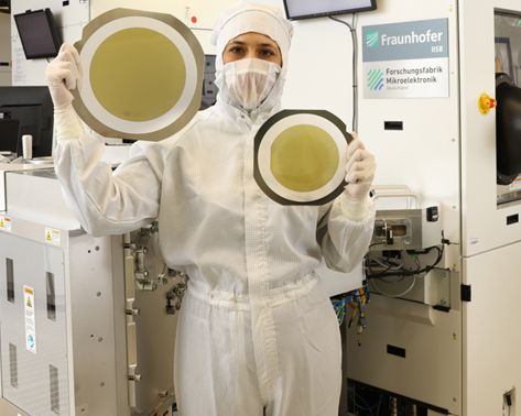
We support material, device and equipment manufacturers and their suppliers by delivering scientific-technological solutions in the field of production and characterization of crystals, epitaxial layers, and devices. This ultimately enables our partners to improve their material quality and reduce production costs. To achieve this, we identify defects that are harmful for the device performance and reliability and look for solutions to avoid them. We develop technologies for new materials and tailor the material properties for new applications. Our focus is on semiconductors for power electronics, communication electronics, sensors, detectors, and quantum technologies.
Strategy
Our strategy is the optimization of the manufacturing processes through a combination of thorough experimental process analysis, tailored characterization techniques, and numerical modeling. For that purpose, we have a well-suited infrastructure at hand, which consists of R&D type furnaces and epitaxial reactors, state of the art metrology tools for the investigation of the physical, chemical, electrical, and structural material properties as well as powerful simulation programs well suited for heat and mass transport calculations. Prototype devices can be processed in house in our qualified 150 mm SiC line or in our flexible R&D line.
Competences
We have profound experience in the areas of semiconductor crystal growth, epitaxy, and device processing including characterization and modeling. In the past, we have significantly contributed to the development of the VGF technique for the industrial production of a variety of crystal materials as well as to the epitaxy of high quality SiC layers. Several national and international research awards underline the achievements of the Materials Department over the last years for its outstanding scientific-technological results as well as for its excellent contributions to the education of students and engineers.
 Fraunhofer Institute for Integrated Systems and Device Technology IISB


