 Fraunhofer Institute for Integrated Systems and Device Technology IISB
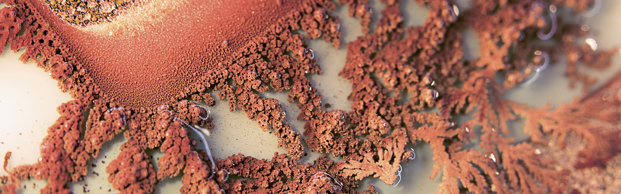
© Grabinger/ Fraunhofer IISB
Materials and Processing
Silver Sintering
- Pressureless and pressure assisted (up to 75kN) process for small and large areas
- Single and double sided semiconductor devices
- Multichip power modules using pre attaching
- Selective sintering on populated circuit boards
- Sintering of active and passive components
- Sintering on DCB, PCB, and leadframe
- Screening of different sinter material
Soldering
- Standard lead free tin based and high temperature alloys
- Void free soldering with paste and preform material
Direct Bonding
Summary:
- No intermediate layer
- Reduced assembly process steps
- Reduced process costs
- Fine pitch
- Very high bonding strength made for power electronics
Research fields
- New materials for bond wires like copper, composites, or alloys
- Improvement of application’s lifetime by bonding parameters, geometry, material, and others
- Metalization and surface optimization of semiconductors for best bondability
- Cleaning process to achieve a reliable bond connection
- In combination with power cycling tests a correlation between bonding parameters to lifetime is possible
- Aluminum and copper wedge-wedge-bonding with diameters from 100μm to 500μm possible
- Ribbon bonding
- Gold ball-wedge bonding with diameters from 25μm to 75μm possible
- Heatable work holder for bond process under temperature for up to 200°C
- Quality assurance through pull and shear tests
- Control of reliability and lifetime by active power cycling test, passive temperature cycling and vibration tests
- Design of experiments to find best suited bonding parameters
Corrosion Effects and Prevention
Corrosion Research and Corrosion Prevention
Corrosion and corrosion protection are being researched at Fraunhofer IISB. Various environmental tests, for example, damp heat tests, temperature shock tests, and corrosive gas tests are conducted. Within the investment program of the German Federal Ministry for Education and Research (BMBF) for microelectronic research, which is called the “Research Fab Microelectronics Germany” (FMD), new equipment and systems are procured. These include a new temperature shock chamber with a wider temperature range and a higher maximum temperature; a corrosive gas test chamber with a higher possible temperature, humidity, and gas concentration; a HAST (highly accelerated stress test) system, also referred to as pressure cooker, for accelerated testing with high humidity, high temperature and air pressure, and a salt spray test chamber.
Testing methods (performed at Fraunhofer IISB)
- Salt spray (e.g. DIN EN 60068-2-52)
- damp heat testing (e.g. DIN EN 60068-2-67)
- thermal shock testing and temperature cycling (e.g. DIN EN 60068-2-14)
- Corrosive gas (H2S, NO2, Cl2, SO2 and mixed gas) (e.g. DIN EN 60068-2-42)
- Highly accelerated stress test (HAST), pressure cooker test (PCT) (e.g. DIN EN 60068-2-67)
- Combined with voltage treatment (power cycling) (e.g. DIN EN 60068-2-67)
Increasing Requirements and Applications under Extreme Environmental Conditions
Due to steadily increasing requirements in terms of higher packaging densities or miniaturization, the problem of electrochemical corrosion is coming more and more to the fore. Furthermore, the demand for using power electronic modules under extreme environmental conditions is rising.
Examples of such applications are inverters in wind turbines, especially offshore ones, or photovoltaic systems. Power electronics installed in trains, for example, need to withstand fast climate changes when driving through a tunnel. This also applies to automotive and telecommunications industries, which serve a worldwide sales market and must ensure the functionality of the electronic components in different climate zones, with high temperature fluctuations and extreme humidity. Most extreme environmental conditions are to be found in the field of aerospace with extreme climate changes, radiation, and mechanical stress. Under the mentioned conditions, condensation resulting from a temperature drop can lead to moisture in the module, for example.
Electrochemical Migration
ECM occurs immediately in electronic packages if there is a gap due to delaminated insulating potting material, metals and metal combinations that tend to corrode, humidity and a sufficient voltage load. Given these conditions, metal ions dissolve and the positive metal ions migrate from the anode to the cathode, where the ions are captured. In this way dendrites grow from the cathode to the anode.
Dendrite growth:
- Potential and humidity between metallic structures is present
- Metal ions dissolve
- Positive metal ions migrate from the anode to the cathode
- Ions are captured at the cathode
- Dendrites grow from the cathode to the anode
Kurt Fuchs / Fraunhofer IISB (Camera / Editing)
Encapsulation Materials and Technologies
As corrosion or rather corrosion resistance is not purely a material property but a system characteristic, the module concept must be considered as a whole. Corrosion behavior and corrosion resistance equally depend on three spheres of influence – the metal, the environment, and the design of the technical system, ranging from the microscopic surface quality and the material combination to the overall concept.
The most obvious measure is to prevent humidity in the module as well as delamination of the coating material. If this cannot be inhibited, it has to be at least delayed. Metal, solder, or other residuals from the production process have to be avoided in or around the insulation gaps. The metals and metal combinations used have to be well chosen, and it is possible to use metallic coatings to prevent corrosion.
The adhesion of the potting has to be long-lasting, at least ensured by an appropriate surface quality of the interface. To achieve this, bonding agents can be used. Polymeric coatings of the metallization (for example polyimide or Parylene) are insulating and can prevent the diffusion of humidity. The whole case of the module can be encapsulated by adhesives and sealed with additional polymer materials to avoid any humidity in the module. Other possibilities are using potting materials with corrosion inhibitors, semipermeable membranes on the interface to the environment, or even hermetic housings with a dry interior.
Parylene Coating
An innovative process for the permanent sealing of electronic assemblies and components is Parylene. In this technique, a transparent polymer film is applied to the substrate in a vacuum by condensation from the gas phase.
The Parylene coating promises resistance to acids and alkalis as well as protection against moisture and dust. Due to the gaseous deposition, the Parylene is able to coat areas and structures which are not or only insufficiently coatable with liquid-based processes. Examples for such areas are sharp edges or tops or narrow and deep gaps. A Parylene coating system is also procured within the investment program FMD of the BMBF.
Inorganic Encapsulation
Inorganic materials and multilayer stacks of organic and inorganic materials offer advanced protection against humidity and hazardous gases. Furthermore the utilization of inorganics allows for superior electrical characteristics with respect to electrical parameters like permittivity, charge/defect densities or suitability for radio frequency operation.