 Fraunhofer Institute for Integrated Systems and Device Technology IISB
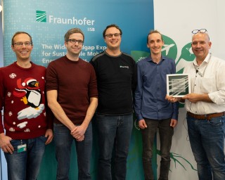
This years Fraunhofer IISB Awards for Research and Development are all about high-performance power electronics for e-mobility.
more info
This years Fraunhofer IISB Awards for Research and Development are all about high-performance power electronics for e-mobility.
more info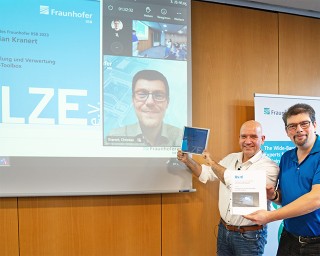
Christian Kranert, Group Manager Equipment and Defect Simulation of the Materials Department at Fraunhofer IISB, developed a new software for the fast, full-wafer and automated detection and classification of crystal defects in silicon carbide (SiC) substrates. He also pushed the licensing of his new, so-called x-ray ropography (XRT) toolbox to the users of the x-ray topography measuring device XRTmicron from Rigaku. Another highlight is the establishment of two new SEMI International Standards for 4H-SiC defect quantification using XRT test methods. These outstanding results confirm the success of the Joint Labs model at Fraunhofer IISB. Joint Labs are an exclusive opportunity to collaborate with Fraunhofer IISB in an industry-compatible laboratory environment.
more info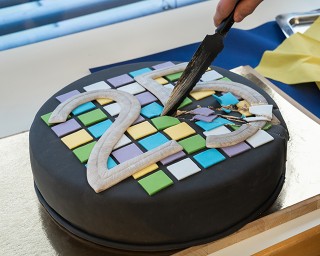
With a delicious wafer-shaped cake and great community spirit we celebrated the 25th workhop of the GMM user group "Deposition and Etch Processing" on Colleagues from the international semiconductor community gathered at the Fraunhofer IISB in Erlangen to discuss current developments in the field of wide-bandgap semiconductor technology and to network. The focus was on new unit processes for deposition and etch. On this festive occasion, Dr. Werner Robl (Infineon Technologies) and Dr. Georg Roeder (Fraunhofer IISB) were honored with uniquely processed jubilee wafers for their dedicaction to keep the GMM user group running since it's first meeting in 1999. Going forward, Dr. Mirko Vogt, Manager Chemical Vapor Deposition at Infineon and Dr. Susanne Oertel, head of the Front End department at Fraunhofer IISB, will take over the organizational activities for the "Deposition and Etch Processing" GMM user group.
more info
A cross-organizational team from Rigaku SE and Fraunhofer IISB has established a new semicon-ductor material characterization method in their jointly operated Center of Expertise for X-ray Topography in Erlangen, Germany. They succeeded not only in developing an industry-ready X-ray topography system, but also in employing defect detection and quantification algorithms, achieving a worldwide unique material characterization method for silicon carbide (SiC) wafers. SiC is an excellent semiconductor for application areas like electric mobility and transportation, sustainable energy supply, industrial infrastructure up to sensors and quantum technologies even under harsh operating conditions. As representatives for the whole research team, Dr. Kranert and Dr. Reimann from Fraunhofer IISB and Dr. Hippler, Managing Director Rigaku Europe SE, have won the Georg Waeber Innovation Award 2023 from the Förderkreis für die Mikroelektronik e.V. (Microelectronics Promotion Society).
more info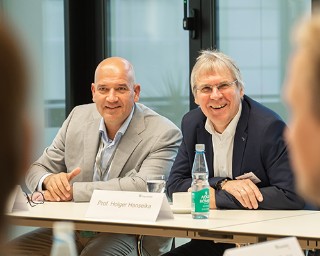
Prof. Holger Hanselka ist seit Mitte August 2023 neuer Präsident der Fraunhofer-Gesellschaft. Seine Dialogtour führt ihn zunächst an fünf Fraunhofer-Standorte, unter anderem nach Erlangen ans Fraunhofer IIS und Fraunhofer IISB.
more info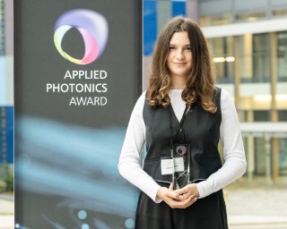
At Photonics Days Jena, Valeriia was handed the award by Prof. Anke Kaysser-Pyzalla, CEO of the DLR (Deutsches Zentrum für Luft-und Raumfahrt e.V.) and Dr. Katja Böhler, State Secretary for Research, Innovation and Economic Development in Thuringia. The Applied Photonics Award is the Fraunhofer IOF's "Young Researchers Award for Innovative Theses" and honors particularly relevant research in the field of applied photonics.
more info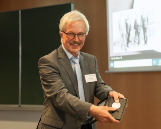
Anlässlich seiner Verabschiedung in den Ruhestand erhielt Dr. Jürgen Lorenz, seit der Institutsgründung 1985 erfolgreicher Leiter der Abteilung Simulation, heute "Modellierung und künstliche Intelligenz", den Fraunhofer-Taler.
more info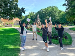
In September, we were once again lucky to welcome new apprentices to our team! We are delighted that we were able to recruit such motivated young people in the areas of microtechnology, IT and office management.
more info
When it comes to particularly low-loss semiconductor components and highly efficient power electronics, there is no way around silicon carbide (SiC) today. The wide-bandgap semiconductor material SiC is superior to conventional silicon in many respects and is conquering more and more new areas of application, for example in optoelectronics, sensor technology or solid-state quantum electronics. Even in space, SiC demonstrates its outstanding physical properties: A SiC UV photodiode from the Berlin-based company sglux is on board the current NASA mission Mars 2020. The SiC chip with the heterostructures for the UV photodiode was processed at Fraunhofer IISB in Erlangen on the institute's own CMOS line. Since the Mars rover “Perseverance” landed on the surface of Mars on February 18, 2021, the SiC photodiode has been functioning with absolute reliability under extreme environmental conditions. The UV sensor is a component of the SHERLOC deep-UV Raman spectrometer, employed by NASA to search for traces of past life on the surface of Mars. Fraunhofer IISB offers SMEs, mid-sized companies and industry low-threshold access to high-tech infrastructure and unique know-how in the field of semiconductor technology.
more info
Semilab is pleased to announce an agreement to form a long-term strategic partnership with Fraunhofer IISB. Within the framework of this cooperation, a demo lab will be opened with a strong focus on developing state-of-the-art metrology and inspection solutions for wide bandgap semiconductor materials.
more info