Characterization
Performance and reliability characterization through measurement of device performance, statistical device reliability predictions considering individual failure mechanisms as well as process evaluation based on yield analysis. Electrical contamination analysis such as carrier lifetime measurements or DLTS for process control or material characterization are being offered in addition.
Contamination Control
In the field of contamination control we are developing or adapting analytical methods and sample preparation methods for the customer-specific cases. More Moore as well as More-than-Moore applications are being addressed. Our focus is the developement of advanced contamination control methods for yield enhancement. Solutions for the characterization of wafers, processes, media, materials, and equipment concerning their contamination behavior, for determining contamination sources, and for certifying cleanroom suitability are being developed together with partners.
Preparation and analysis of nanostructures with the Focused Ion Beam (FIB)
With our dual-beam systems consisting of a scanning electron microscope (SEM) and a focused ion beam (FIB), we process and image any materials simultaneously and with nanometer precision. This allows us to analyze defects in assembled systems, visualize doping and damage processes in implanted devices, analyze cross-sections in a layered system or perform local process control on wafers. Our decade-long experience with a wide variety of materials opens up a long list of preparation and analysis options from semiconductor materials to polymers, glasses, diamonds, bones, metals, crystals, ceramics, ...
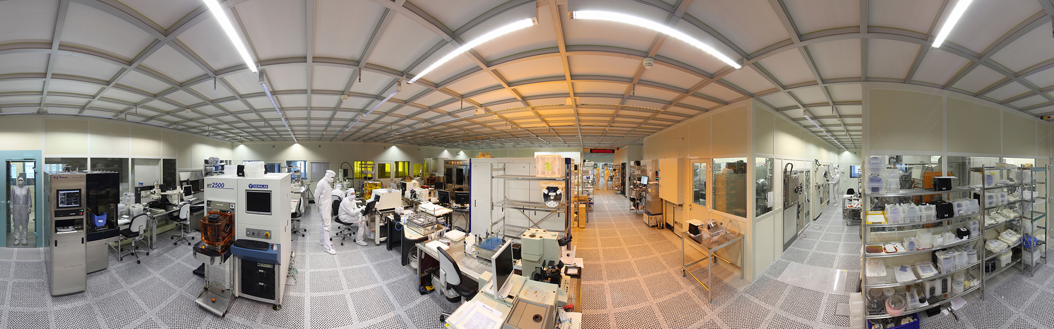
 Fraunhofer Institute for Integrated Systems and Device Technology IISB