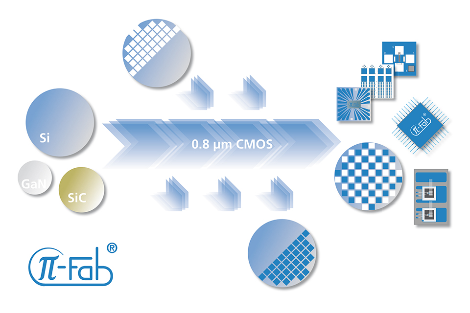
The unique characteristic of π-Fab is a high flexibility in wafer material and size. Silicon wafers with diameters of 150 mm and 200 mm are handled by default, further diameters on request. The process line is based on a 0.8 μm Si-CMOS technology. To keep flexibility high an advanced contamination control is available.
SiC Prototype Foundry
Special attention has been given to silicon carbide (SiC) device processing on 150 mm wafers. In order to realize all dedicated SiC process steps, such as epitaxy, ICP dry trench etching, growth of silicon dioxide, implantation at elevated temperatures, implant activation annealing, or ohmic contact alloying, we provide additional equipment.
Furthermore, π-Fab is designed as a platform where equipment assessment and optimization, or manufacturing control issues for customers can be covered. It thus also forms the basis for IISB’s SiC-Services, which cover the whole value chain, from material to devices, SiC modules development and assembly up to implementation of SiC mechatronic systems.
Available Process Steps
As described above, π-Fab sums up to flexibility and individuality and handles various wafer sizes and types. As of that, it is our main objective to support our customers with the fabrication of customized electron devices, as well as with particular processing steps or combination of steps, while enabling the customer to determine the points of entry and exit from the process line, at any time:
 Fraunhofer Institute for Integrated Systems and Device Technology IISB