 Fraunhofer Institute for Integrated Systems and Device Technology IISB
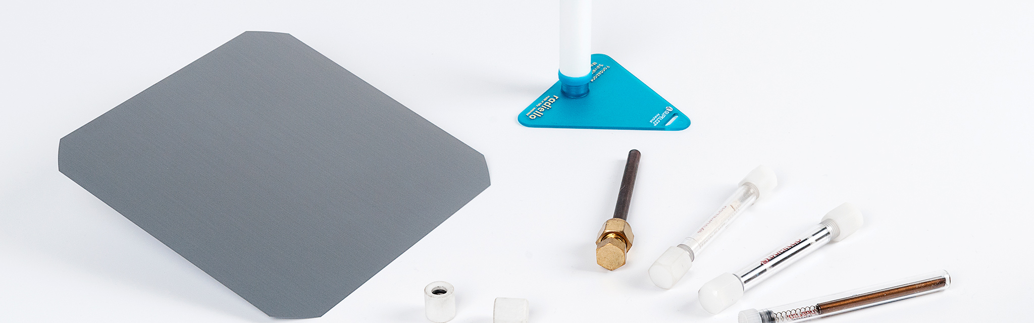
Research Topics
In the field of contamination control we are developing or adapting analytical methods and sample preparation methods to provide emerging solutions for our partners. More Moore as well as More-than-Moore applications are being addressed. With feature sizes shrinking, thinner layers, new materials, 3D integration and more complex designs, contamination control is a constant challenge and a prerequisite for a continuous quality control and achieving high yields in the manufacturing processes.
Our focus is the developement of advanced contamination control methods for yield enhancement. Solutions for characterizing wafers, processes, media, materials, and equipment concerning their contamination behavior, for determining contamination sources, and for certifying cleanroom suitability are being developed together with partners. The characterization methods include the analysis of organic, inorganic and particulate contamination.
Furthermore, a test capabilities for the assessment of sensors or other electronic systems under various atmospheric conditions -even evaluations in harmful atmospheres - are being developed.