Wide-bandgap power at silicon cost – YESvGaN project
develops competitive GaN process technologies
Can we contribute to the worldwide energy challenge by maximizing the efficiency in power conversion at a low cost? The answer is: YESvGaN! So, the goal of the YESvGaN consortium is to create a new class of vertical power transistors based on gallium nitride (GaN), so-called vertical GaN membrane transistors. These novel power devices combine the efficiency of wide-bandgap (WBG) semiconductors with the lower cost of the established silicon semiconductor technology. Within YESvGaN, the development of the required new technology all the way from wafer to application is covered.


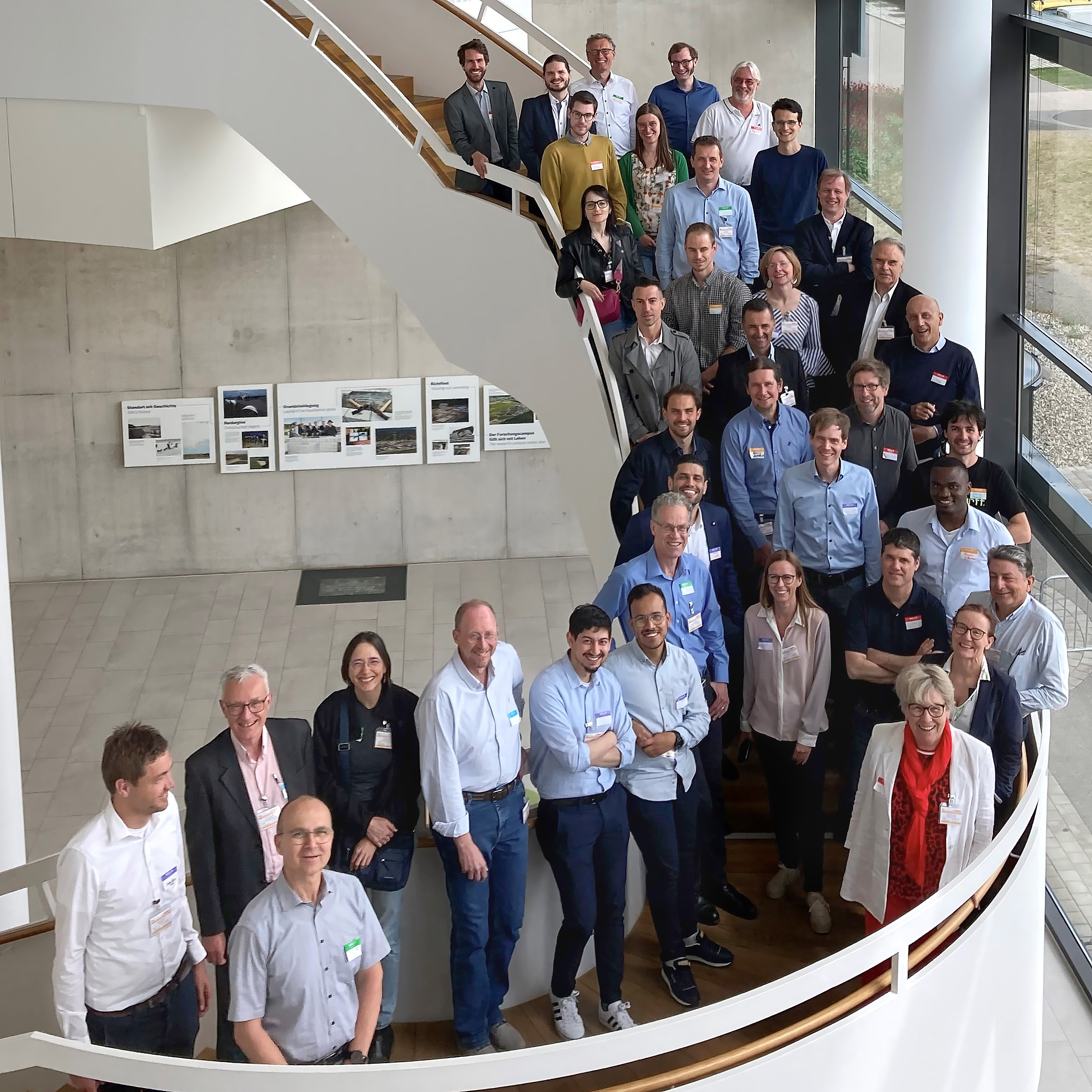
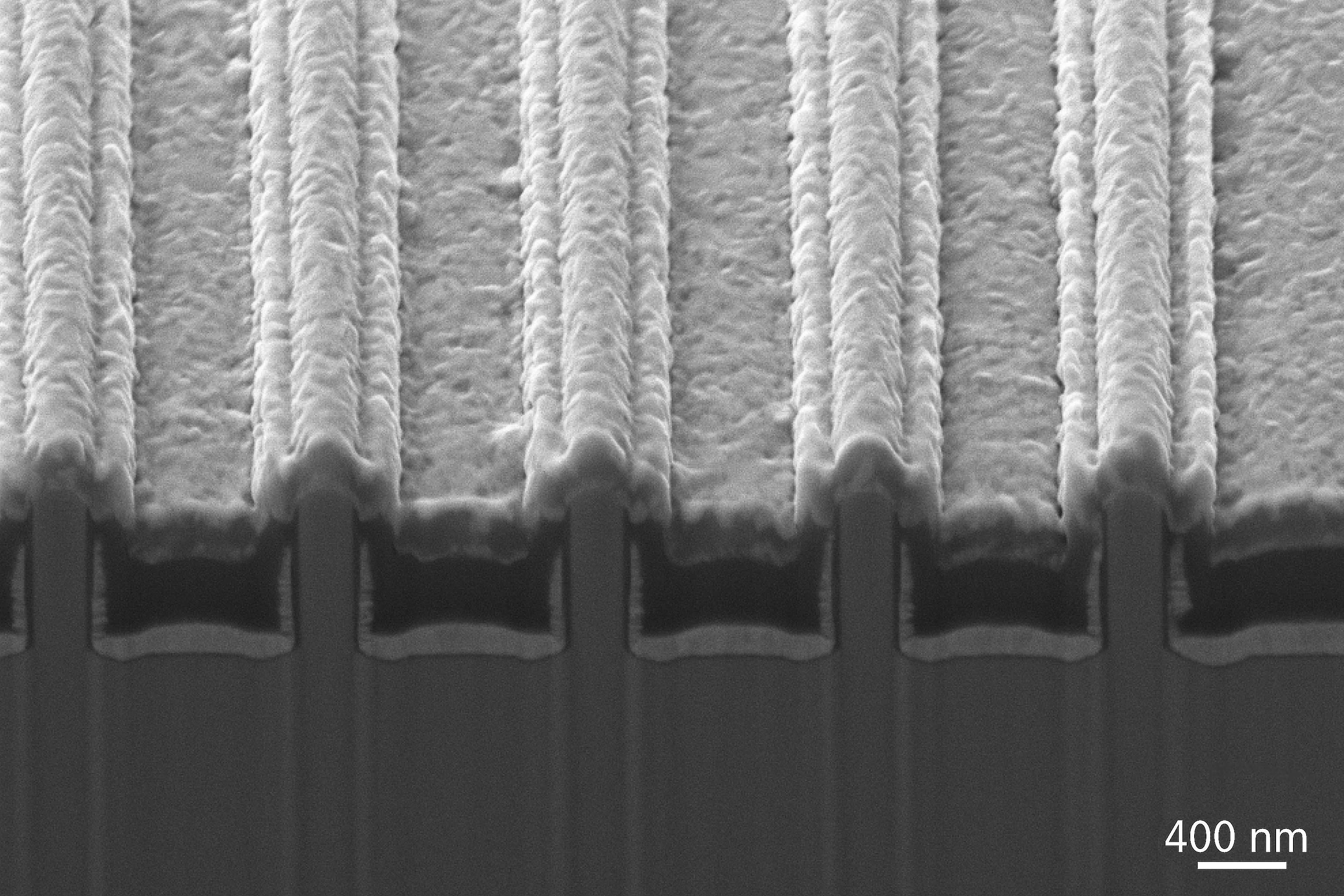
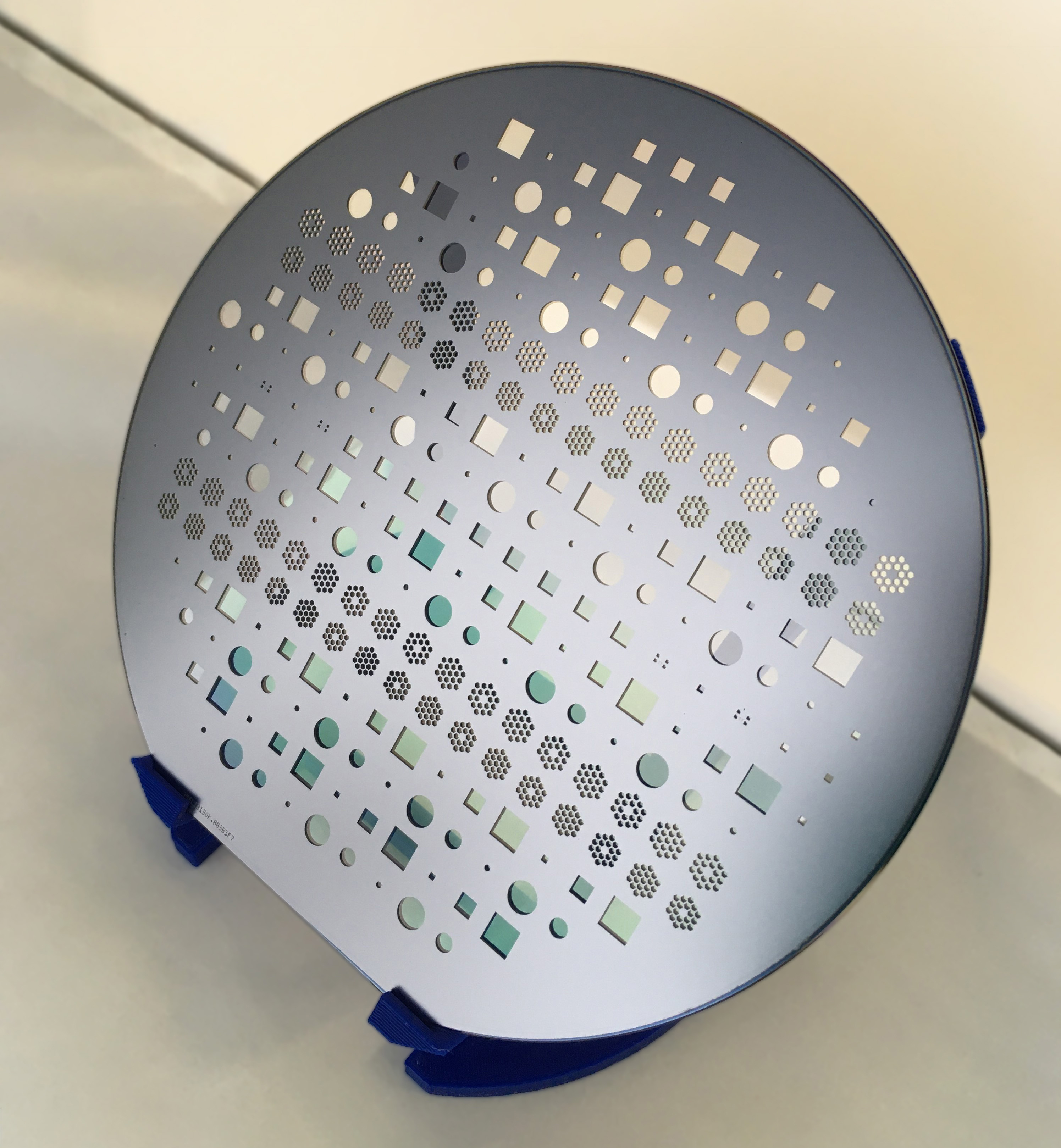
Since the project launched on May 1, 2021, impressive developments have been made by the project consortium, consisting of 23 European partners. Vertical device demonstrators with FinFET architectures and Schottky diodes – being important building blocks for a novel vertical membrane transistor technology – have been created successfully. Also, vertical layer stacks have been grown on silicon and sapphire with a diode breakdown voltage exceeding 500 V. This is a major step to reach the overall project goal of 1200 V blocking voltage on low-cost silicon or sapphire substrates. As a result, the market for future high-performance applications, e.g., in the automotive industry, could be accessible for the GaN semiconductor material.
For vertical GaN power transistors with ultra-low resistance contribution from the backside contact, the development of a reliable membrane process technology is crucial. YESvGaN has succeeded in producing such fragile GaN membranes with a thickness of a few micrometers and a diameter of several millimeters without breaking. Novel assembly and interconnection technologies are being tested for the final application of membrane vertical GaN power transistors under extreme conditions. This includes operating temperatures of more than 250 ⁰C. In addition, virtual prototypes are being developed to evaluate the efficiency of GaN devices in the target applications using digital twins.
We are confident that YESvGaN will continue to achieve promising results in the next phases of the project and take a significant step towards fully vertical GaN membrane transistors. So, can we contribute with energy-efficient low-cost vertical GaN technology to the worldwide energy challenge? Our answer remains: YESvGaN!
About YESvGaN
The ECSEL-JU funded YESvGaN project was launched on May 1, 2021. The YESvGaN consortium consists of 23 partners, featuring strong collaborations between academia and industry among seven different European countries.
Contact
Project Coordinator: Dr. Christian Huber, Robert Bosch GmbH
Dissemination Manager: Dr. Sofie Vandenbroucke, Ghent University
Project Office: Joachim Mertz, K&S GmbH Projektmanagement
E-Mail: info@yesvgan.eu
For more information about the YESvGaN project, see www.yesvgan.eu.
Follow our latest project activities on LinkedIn and Twitter.
About Fraunhofer IISB
Intelligent Power Electronic Systems and Technologies - according to this motto, the Fraunhofer Institute for Integrated Systems and Device Technology IISB, founded in 1985, conducts applied research and development for the direct benefit of industry and society. With scientific expertise and comprehensive systems know-how, the IISB supports customers and partners worldwide in transferring current research results into competitive products, for example for electric vehicles, aviation, production, and energy supply.
The institute consolidates its activities in the two major business areas of Power Electronic Systems and Semiconductors. In doing so, it comprehensively covers the entire value chain from basic materials to semiconductor device, process, and module technologies to complete electronics and energy systems. As a unique European competence center for the semiconductor material silicon carbide (SiC), the IISB is a pioneer in the development of highly efficient power electronics even for the most extreme requirements. With its solutions, the IISB repeatedly sets benchmarks in energy efficiency and performance. By integrating intelligent data-based functionalities, new use cases are continuously emerging.
The IISB employs about 300 people. Its headquarters are in Erlangen, with additional branches at the Energie Campus Nürnberg (EnCN) and the Fraunhofer Technology Center High Performance Materials (THM) in Freiberg. The institute closely cooperates with Friedrich-Alexander-Universität Erlangen-Nürnberg (FAU) and is a founding member of the EnCN as well as the Leistungszentrum Elektroniksysteme (LZE). In joint projects and associations, Fraunhofer IISB collaborates with numerous national and international partners.
Downloads / Links
Last modified:
 Fraunhofer Institute for Integrated Systems and Device Technology IISB