 Fraunhofer Institute for Integrated Systems and Device Technology IISB
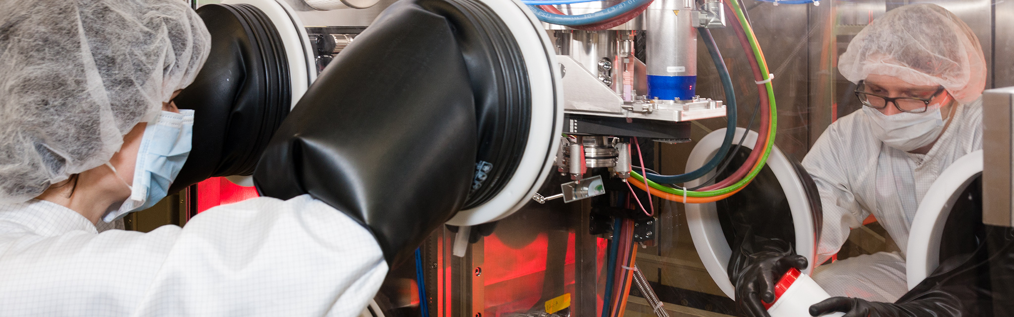
We develop the HVPE growth of GaN bulk crystals up to 4“ diameter. The process is optimized towards a high uniform V/III ratio along the growing interface by comparing in-situ process data, ex-situ determined properties of the crystal with results from numerical modeling of the growth process. We pioneer the PVT growth of AlN crystals by using our unique N-face technology. The focus is on deeper understanding of growth mechanisms and upscaling towards 2” diameter. In our wafering line we explore advanced GaN and AlN crystal preparation technologies for epi-ready wafers. These wafers are used in our R&D clean room line to process prototype devices for fast feedback on material quality.
© Anja Grabinger / Fraunhofer IISB

© Anja Grabinger / Fraunhofer IISB
GaN & AlN

Synchrotron White Light Topography "SWBXRT"

AlN Crystal
AlN wafer
Services
- Growth of GaN and AlN crystals
- Epitaxy of AlGaN on GaN, AlN and sapphire substrates up to 4” diameter
- Simulation of heat and mass transport of the HVPE and PVT process
- Identification of device critical defects in nitrides
- Characterization of crystals and epitaxial structures
- imaging of extended defects by x-ray topography
- defect selective etching
- Cathodoluminescence
- Photoluminescence
- Raman- and FTIR spectroscopy
- Investigation of electrical properties of extended defects by conductive atomic force microscopy and electron beam induced current measurements and imaging techniques
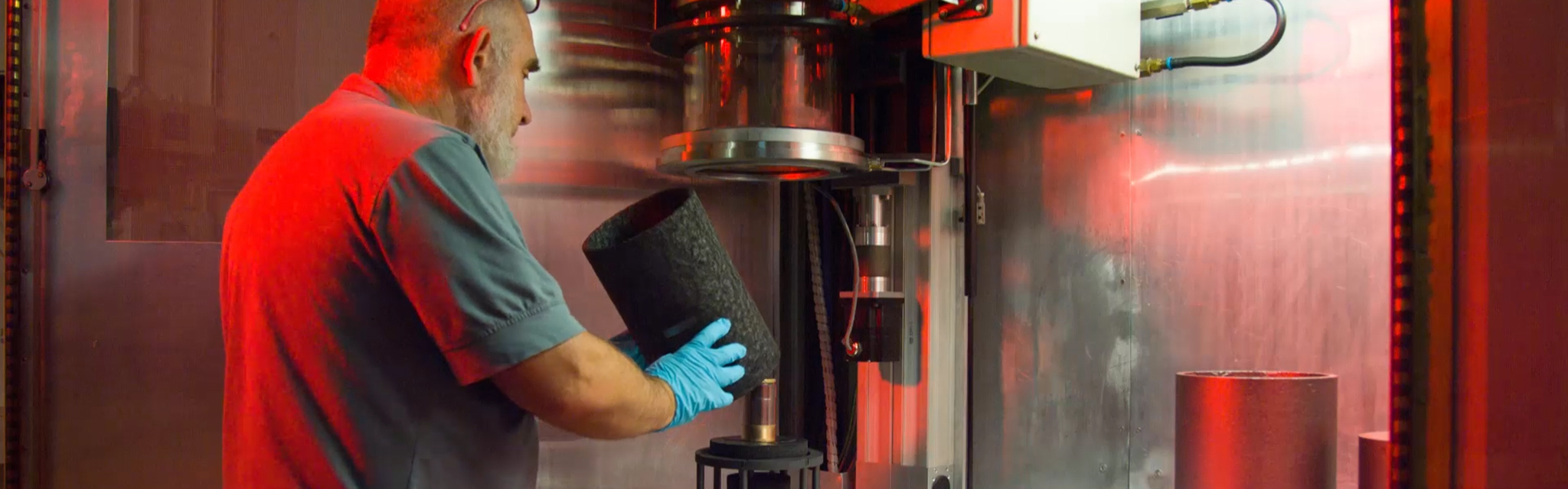
Mounting of a GaN sample in a special furnace for defect selective etching

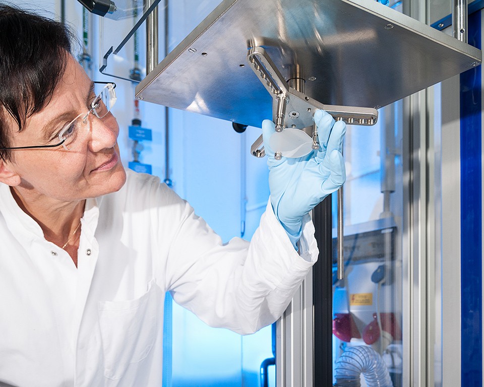
Fraunhofer IISB is equipped with a wafering laboratory for cutting GaN & AlN crystals into wafers.

The epi ready quality of GaN & AlN wafers after grinding, polishing and cleaning is controlled in house by AlGaN epitaxy up to 1450°C.
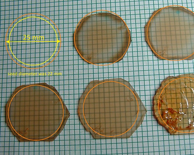
First Aluminum Nitride Crystal with 43 mm Diameter and 1-inch Aluminum Nitride Wafers

First aluminum nitride crystal with 43 mm diameter grown at Fraunhofer IISB

Polished and finished 1-inch AlN Wafer
In 2022, we succeeded in growing a 43 mm diameter aluminum nitride (AlN) crystal with a diameter of 43 mm in technology-relevant quality. In March 2023, we have taken the next step and processed the first 1-inch AlN wafers from this crystal.
The availability of AlN crystals respectively AlN wafers in sufficient size and quality is the key for the manufacturing of high performance AlN-based electronic devices. Aluminum nitride as a semiconductor offers an extreme breakdown field strength, a high material quality, a low amount of defects and a very good thermal conductivity.
Due to the special physical properties of AlN, AlN-based devices for power electronics can achieve a performance beyond that of silicon carbide (SiC) and gallium nitride (GaN). Thus, AlN is suitable for the processing of super-low loss power transistors and has the potential to become the most important Ultra Wide Band Gap (UWBG) semiconductor for power electronics in the future.
For our institute, this result is a substantial step to reach the important milestone inside the BMBF funded project LeitBAN. This achievement was possible by the support of the BMBF FMD initiative.
YESvGaN – GaN Vertical Power Transistors at Silicon Cost

Free and intact GaN membranes on a Si carrier wafer.
YESvGaN targets a new low-cost wide-bandgap (WBG) power transistor technology for enabling high-efficiency power electronic systems for electromobility, industrial drives, renewable energies, and data centers.
The main objective of the project is to demonstrate innovative vertical gallium nitride (GaN) power transistors fabricated on a low-cost substrate such as silicon. This so-called vertical membrane architecture combines the superior performance of GaN as WBG power transistor material with the advantages of a vertical architecture regarding current and voltage robustness at a price competitive to silicon IGBTs. Within YESvGaN, the entire value chain is addressed – from substrate, epitaxy, process, and interconnect technology to applications in power electronic systems. The YESvGaN consortium combines the experience and competence of 23 industrial and research partners from 7 European countries.
Fraunhofer IISB contributes to the project along the entire value chain, including:
- Analysis of epitaxial layer stacks and crystal defects, development of innovative routines for measuring the electrical properties of defects and thin membranes
- Definition of new processes for handling of thin membranes during packaging and ceramic embedding
- Electrical characterization of novel power devices, development of an electrical simulation model, and design of a half-bridge power module
Press release about the latest project developments (Nov. 2022)
Innovative Reliable Nitride based Power Devices and Applications
Fraunhofer IISB is partner in the large highly visible EU research initiative "InRel-Power"