 Fraunhofer Institute for Integrated Systems and Device Technology IISB
We are experienced with the characterization of the optical, electrical, structural, physical, and chemical properties of different crystal, wafer and epi materials as well as of partially and fully processed devices. This allows us on the one hand to perform service measurements within a fast return time for our customers. On the other hand we use this toolbox, especially our in-house epi reactors in combination with the possibility to process test devices, to identify defects critical for device performance and reliability, to understand their origin and to find solutions together with our customers how to overcome the critical defects.
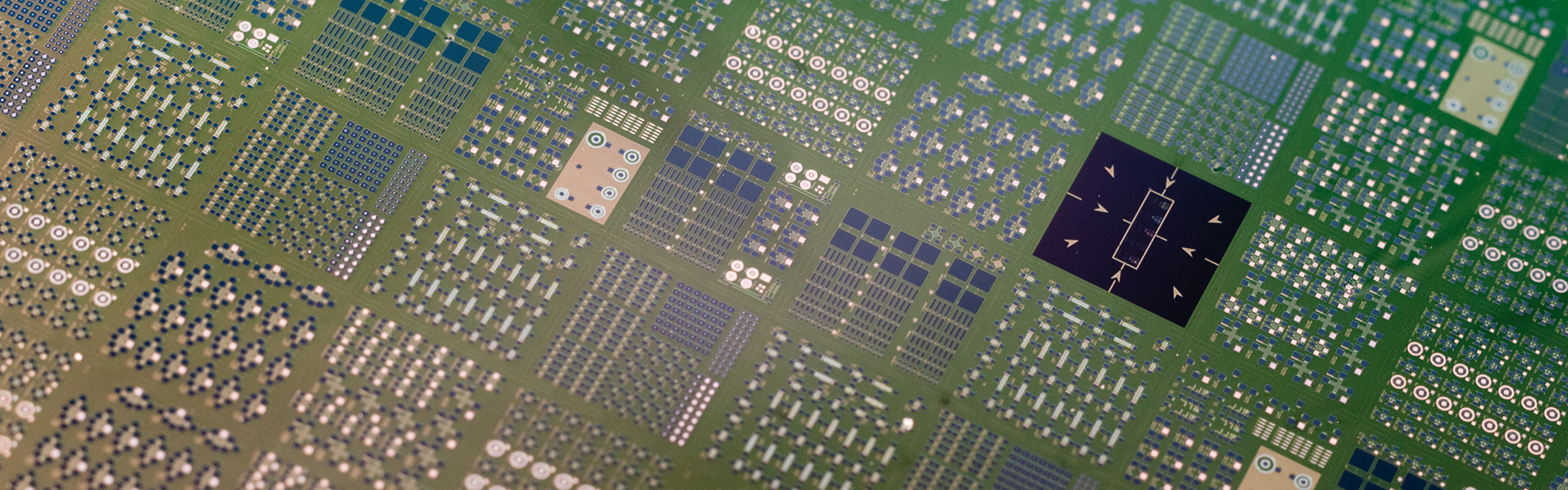
© Thomas Richter / Fraunhofer IISB
Material Analysis
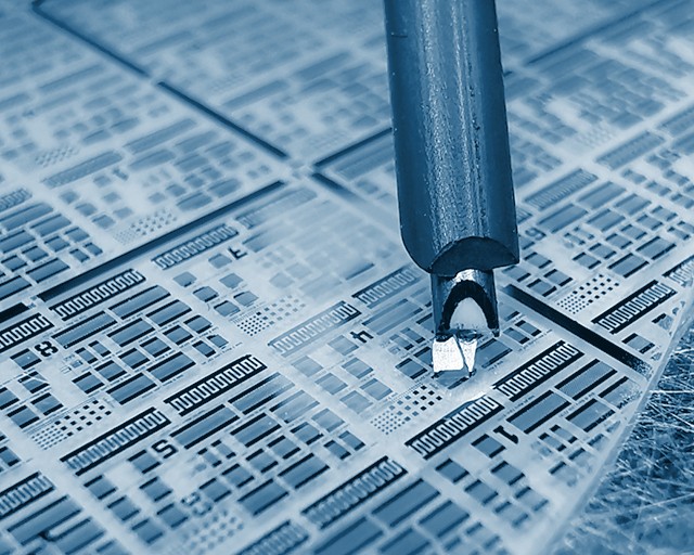
SAW structures on sapphire

Optical and electron microscopy
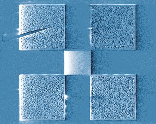
EBIC image of GaN HEMT device
Services
- Identification of device critical materials defects
- Epitaxy (SiC, AlGaN) and device processing
- Characterization of crystals, epitaxial structures and devices
- x-ray topography, x-ray diffraction
- optical microscopy, scanning and transmission electron microscopy
- various atomic force microscopy methods
- LPS to determine interface shapes
- electrical and optical defect spectroscopy like
- DLTS, optical DLTS
- cathodoluminescence, photoluminescence
- PL scanner for full wafer imapging
- EBIC, Raman- and FTIR spectroscopy
- minority lifetime measurements (µPCD, MDP)
- IV & CV measurements, and much more
- Development of tailored metrology tools together with metrology manufacturer