 Fraunhofer Institute for Integrated Systems and Device Technology IISB
Joint Labs offer industry the opportunity to collaborate with Fraunhofer IISB in form of a cross-organizational development team, which works together on the industry's key topics. This promotes a deeper understanding of the technology, which in turn facilitates technology transfer and accelerates integration into the product. To enable the team to work together successfully, premises are provided for the interdisciplinary team and the correspondingly necessary technical infrastructure, in which the team members can work together on the problems and develop new technologies and products. The Joint Labs can also function as a demo and application center for newly developed tools and equipment.

© Kurt Fuchs / Fraunhofer IISB
Joint Labs
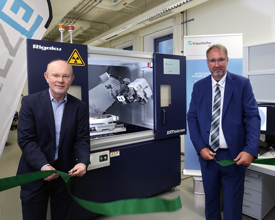
Inauguration of the Center of Expertise for X-ray topography together with Rigaku Corporation
Team of the Joint GaN HVPE Lab built together with Freiberger Compound Materials

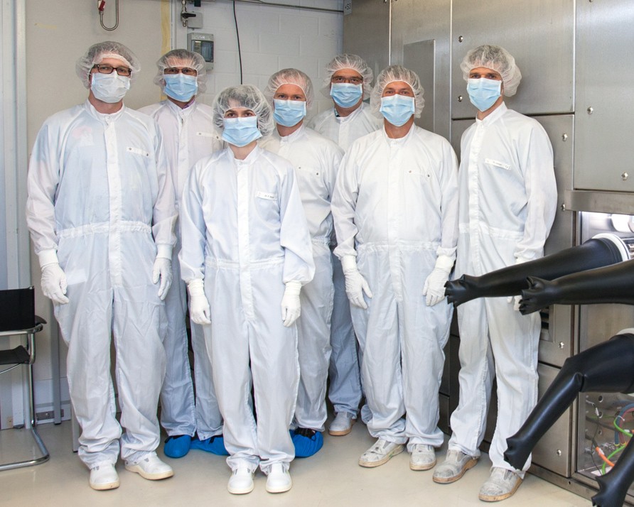
Insight in the 200 mm SiC Epitaxy Demolab built together with Aixtron SE
Examples
Based on the worldwide recognized expertise of Fraunhofer IISB in SiC epitaxy technology and characterization, the SiC Epitaxy Demolab will jointly enable the optimization of epitaxial production processes for 150 and 200 mm SiC wafers using Aixtron´s state-of-the-art G5WW production tools. The goal of the collaboration is the demonstration of efficient and economic high-volume manufacturing processes addressing the SiC material requirements of SiC power devices.
Rigaku Corporation and Fraunhofer IISB have built the Center of Expertise for X-ray Topography in Erlangen to support the semiconductor industry worldwide in improving and better understanding their wafer quality and yield by employing the Rigaku XRTmicron advanced X-ray topography tools. One aim is to develop industrial applicable measurement routines and defect counting algorithms which can be used in production and for R&D purposes.
The Joint GaN HVPE Lab together with Freiberger Compound Materials enables an efficient technology development by combining the know-how for HVPE processes and production equipment with material defect and characterization knowledge to fulfil the needs on material quality of future GaN markets.
Center of Expertise for X-ray Topography
In the Center of Expertise for X-ray Topography at Fraunhofer IISB, we investigate crystallographic defects on wafer scale, non-destructively, with high measurement speed and highest spatial resolution. The X-ray topography measurement method used for this purpose is ideally suited for the analysis of epilayer structures, wafers, wafers with epilayer structures and partially processed wafers.
© Kurt Fuchs / Fraunhofer IISB
Our services:
- Test measurements and tool demonstration
- Development of detailed XRT-measurement-und defect quantification routines incl. statistical defect analysis
- Validation of XRT-measurement results with different characterization methods or industrial in-line tools
- Service based measurement with feedback loops within a few days
- R&D project collaboration
You benefit from our full-surface and non-destructive method as well as feedback loops within a few days. Our experts analyze your samples to support you in quality assurance during your production process or in R&D tasks. This may involve very local defect analysis, for example. We also provide the generation of statistical measurement data based on a large number of wafers to control your material quality on the entire wafer area during ongoing production. The amount and different types of dislocations, slip lines, dislocation networks, (small-angle) grain boundaries, inclusions, precipitates, scratches, bends, etc. are mapped and quantified on the samples.
We use fast, high-resolution XRTmicron X-ray topography systems from our strategic partner Rigaku. These systems are characterized in particular by the different X-ray sources copper, molybdenum, silver and chromium. In combination with the application of large angle goniometers, a wide range of diffraction conditions is possible. Therefore, the X-Ray topography method is suitable for different types of single crystalline materials:
- Semiconductors: Si, Ge, diamond, SiC, GaN, AlN, GaAs, InP, CdTe, CdZnTe
- Oxides: sapphire, ruby, garnets, vanadates, niobates, quartz
- Halogenides: fluorides, bromides
The XRTmicron systems used can be operated in both transmission and reflection mode. This allows defects in the volume of the sample to be detected or near-surface defects to be quantified. Furthermore, the X-ray systems are equipped with a standard and a high-resolution XTOP CCD camera. This results in a spatial resolution of 5.4 µm and 2.4 µm per pixel, with a single image size of 18 mm x 13.5 mm. Full wafer mappings and detailed defect imaging of regions of interest are possible under various diffraction conditions for sample sizes up to 300 mm in diameter. The systems are equipped with a special slit arrangement to perform high-resolution cross-sectional topography measurements with 3D defect reconstruction. Through this process we provide detailed depth information over the entire thickness of your sample.