X-ray Topography

With our XRTmicron topography tools, we investigate crystallographic defects on a wafer scale, non-destructively, with high measurement speed and the highest spatial resolution. The X-ray topography measurement method used for this purpose is ideally suited for the analysis of epilayer structures, wafers, wafers with epilayer structures and partially processed wafers.

Our services:

  • Test measurements and tool demonstration
  • Development of detailed XRT-measurement-und defect quantification routines incl. statistical defect analysis
  • Validation of XRT-measurement results with different characterization methods or industrial in-line tools
  • Service-based measurement with feedback loops within a few days
  • Custom-specific feedback loops within a few days
  • R&D project collaboration

Typical application examples collected with XRTmicron

Defect visualization and quantification for 4H SiC substrate for power electronic application:
X-ray transmission topogram of the 101 reflexes for a full 100 mm 4H SiC wafer.
Surface damage on as-cut AlN substrates for UV-LEDs:
X-ray transmission topogram of the 100 reflexes for a 1" AlN wafer.
Slip-line detection in 200mm silicon:
Detailed X-ray transmission topogram of the 400 reflex for a specific area of a 200mm Si wafer where slip-lines can be seen.

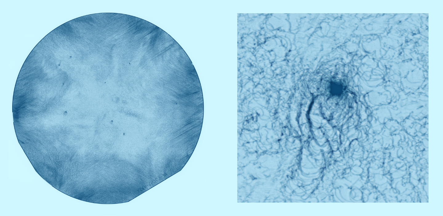
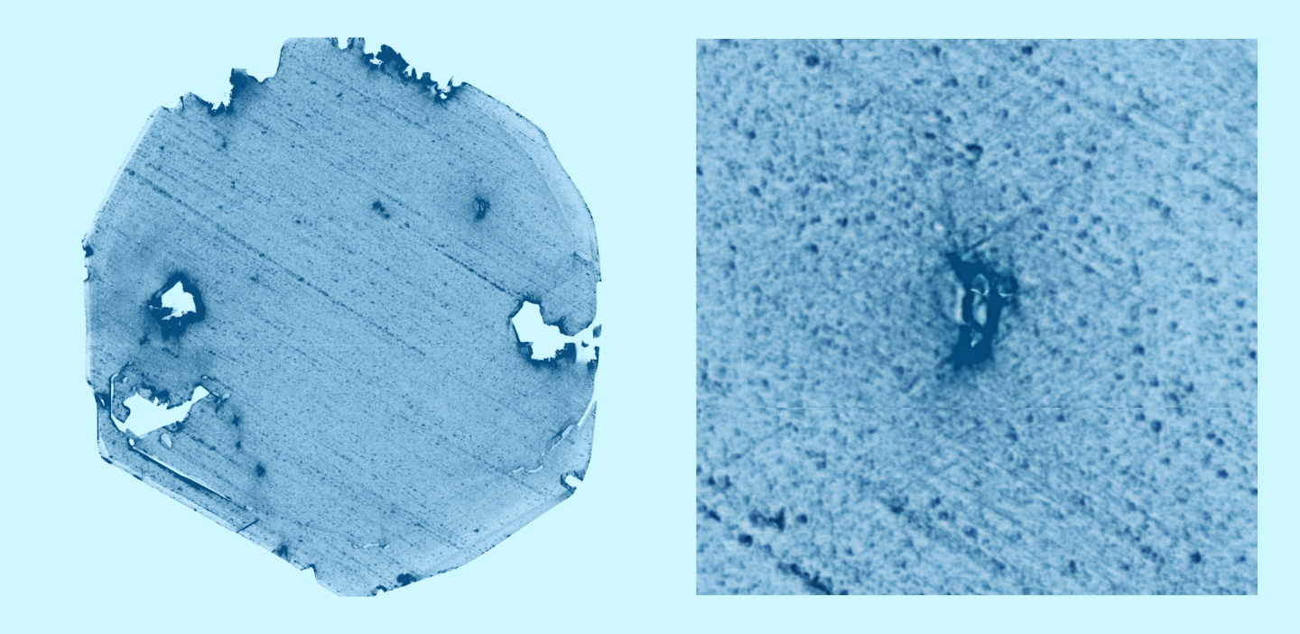
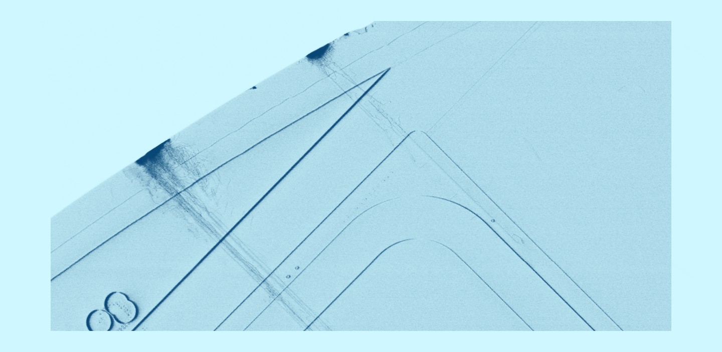
You benefit from our full-surface and non-destructive method as well as feedback loops within a few days. Our experts analyze your samples to support you in quality assurance during your production process or in R&D tasks. This may involve very local defect analysis, for example. We also provide the generation of statistical measurement data based on a large number of wafers to control your material quality on the entire wafer area during ongoing production. The amount and different types of dislocations, slip lines, dislocation networks, (small-angle) grain boundaries, inclusions, precipitates, scratches, bends, etc. are mapped and quantified on the samples.

We use fast, high-resolution XRTmicron X-ray topography systems from our strategic partner Rigaku. These systems are characterized in particular by the different X-ray sources copper, molybdenum, silver and chromium. In combination with the application of large-angle goniometers, a wide range of diffraction conditions is possible. Therefore, the X-ray topography method is suitable for different types of single crystalline materials:

  • Semiconductors: Si, Ge, diamond, SiC, GaN, AlN, GaAs, InP, CdTe, CdZnTe
  • Oxides: sapphire, ruby, garnets, vanadates, niobates, quartz
  • Halogenides: fluorides, bromides

The XRTmicron systems used can be operated in both transmission and reflection modes This allows defects in the volume of the sample to be detected or near-surface defects to be quantified. Furthermore, the X-ray systems are equipped with a standard and high-resolution XTOP CCD camera. This results in a spatial resolution of 5.4 µm and 2.4 µm per pixel, with a single image size of 18 mm x 13.5 mm. Full wafer mappings and detailed defect imaging of regions of interest are possible under various diffraction conditions for sample sizes up to 300 mm in diameter. The systems are equipped with a special slit arrangement to perform high-resolution cross-sectional topography measurements with 3D defect reconstruction. Through this process we provide detailed depth information over the entire thickness of your sample.

Center of Expertise for X-ray Topography

Rigaku Corporation and Fraunhofer IISB built the Center of Expertise for X-ray Topography in 2021 in Erlangen. This strategic joint lab supports the semiconductor industry in improving and better understanding their wafer quality and yield by employing the Rigaku XRTmicron advanced X-ray topography tools.

In our video below we provide insights into the set-up, the inauguration and the activities of the Center of Expertise for X-ray Topography.

© Kurt Fuchs / Fraunhofer IISB

From Lab to Fab - High Throughput and Non-destructive Full Wafer BPD Detection for Silicon Carbide

On our XRTmicron system from Rigaku, we quantify the basal-plane dislocations (BPD) of a whole 150 mm SiC wafer in about 5 minutes and in about 7 minutes for a whole 200 mm SiC wafer. This high throughput non-destructive BPD detection now enables inline defect metrology for SiC wafers on fab-level.

© Elisabeth Iglhaut / Fraunhofer IISB

BPDs are tightly correlated to the thermoelastic stress during SiC crystal growth. A high BPD density in the substrate increases the risk of yield loss during device processing and is an important parameter for wafer quality assessment. The BPD density contains highly valuable information about the crystal quality and the quantification of BPDs allows conclusions to be drawn about the SiC crystal growth process.

The XRT measurement method in general can be applied independent of sample properties like surface polarity and dopant concentration. The new approach is highly tolerant with respect to lattice curvature and slight wafer misalignment, which opens the possibility of reducing the alignment procedure to the mechanical alignment based on the wafer flat or notch.

Read our press release on the inauguration of the Center of Expertise for X-Ray Topography, our joint lab with Rigaku, in 2021:


Download the Brochure on Advanced X-ray Topography: