 Fraunhofer Institute for Integrated Systems and Device Technology IISB
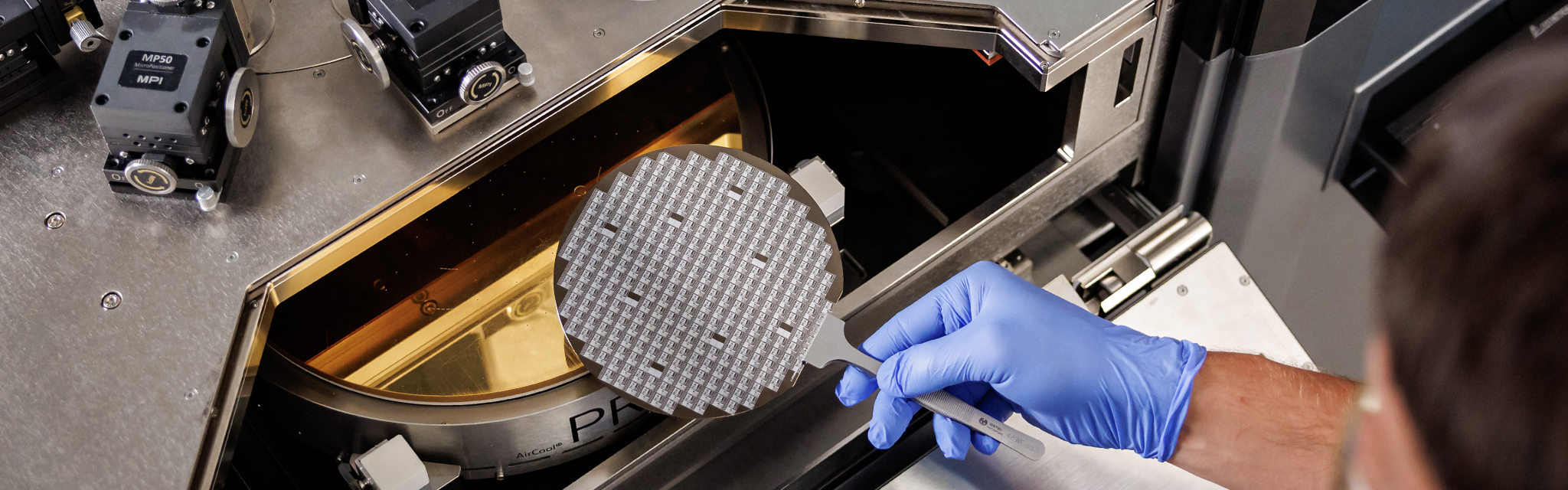
Based on a comprehensive defect-spectroscopic characterization of semiconductor materials (notably GaN, SiC, AlGaN, AlN, GaAs, and InP), test devices can be produced and characterized at an early stage of material development in partnership with the Institute of Applied Physics at TU Bergakademie Freiberg. This facilitates a systematic correlation between material properties and the resulting device characteristics, as well as the identification of defects critical to the devices.
Additionally, the IISB branch in Freiberg allows for addressing custom queries related to process development and the design of test devices. In our flexible, fully CMOS-integrated cleanroom facility, we can both individually adapt processes and correlate material properties with device performance to identify critical material defects.


