 Fraunhofer Institute for Integrated Systems and Device Technology IISB
We are well experienced in the growth and characterization of a variety of other semiconductor materials (Ge, GaAs, InP, CdTe) as well as of optical, laser and scintillator crystals (sapphire, LSO, YVO4, Y2O3, CaF2, CeBr3) by different melt and solution growth techniques such as Bridgman, VGF or THM. We support our customers in the development of crystal growth and epitaxy equipment and processes based on our broad material expertise and by numerical simulation. Furthermore, we offer specific characterization services of crystal and wafer material.
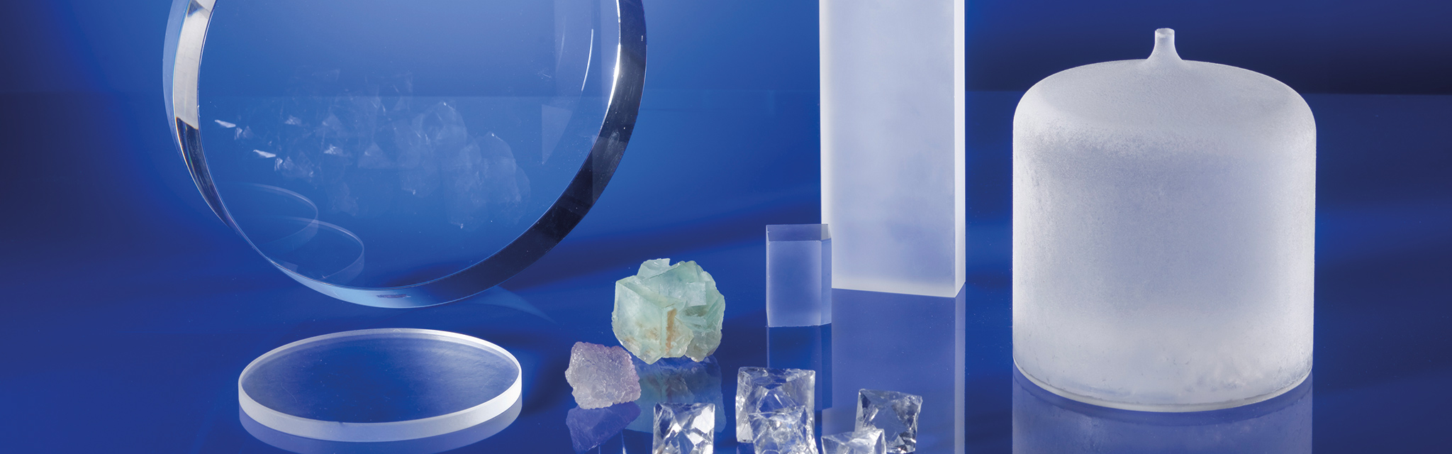
Other Crystal Materials
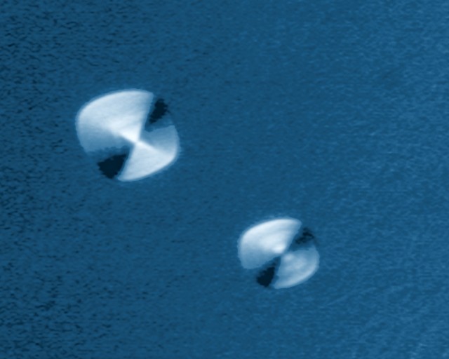
Solid-liquid interface shape in VGF GaAs

VGF crystal growth furnace
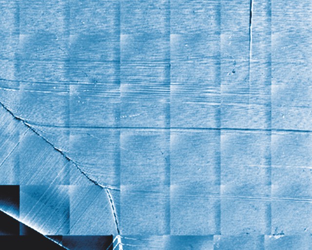
Etch pits on VGF InP sample
Services
- Support of the development of crystal growth and epitaxy equipment by using thermal modeling and our expertise in the engineering of in-situ measuring techniques
- Specific crystal growth experiments in special R&D furnaces in house and at partners’ sites
- Sample preparation for the analysis of the properties of the materials
- Characterization of structural, optical, physical, chemical, and electrical properties
- Simulation of heat and mass transport phenomena including the effects of magnetic fields

Material test equipment for production of scintillator crystals

Polishing and defect selective etching for analysis of the structural properties of compound semiconductor samples

Analysis of crystals and wafers by confocal laser microscopy