Failure Analysis

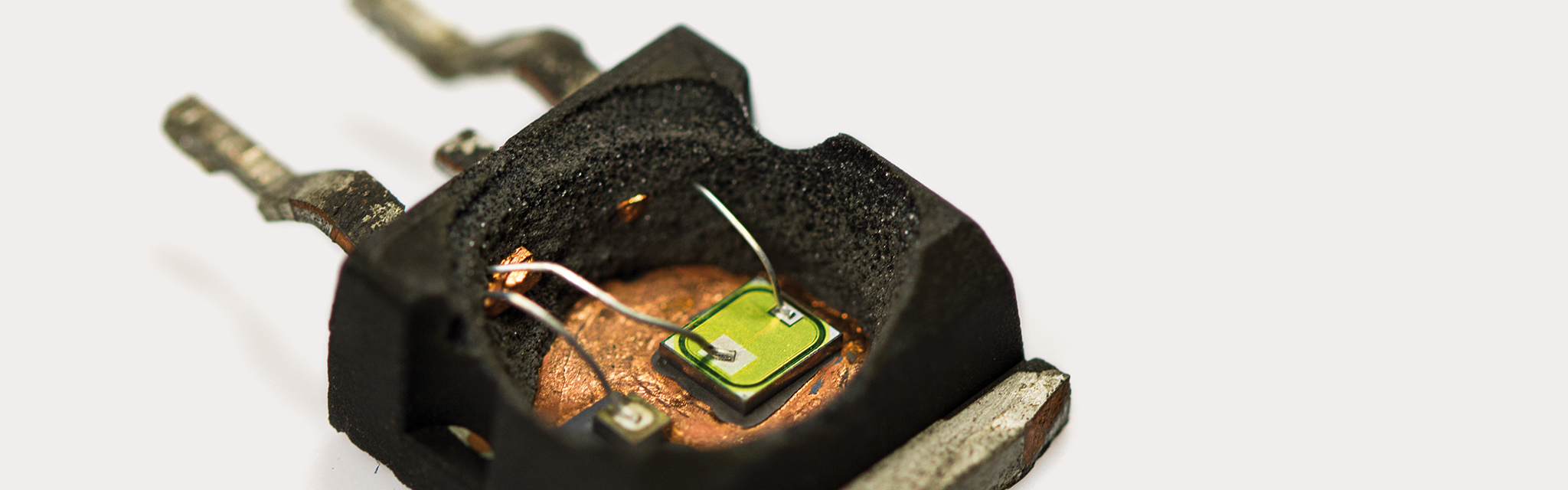
Fields of research and service

  • Investigation of field returns
  • Characterization of samples accompanying in-house and external life time tests such as active power cycling
  • Analysis of new packaging concepts and joining technologies, for instance sinter technology versus soldering
  • Competitive analysis of power electronic systems, modules and devices like power electronics of hybrid vehicles
  • Physics of failure analysis, material characterization for parameterization of existing life time models or enhanced ones
  • Interpretation of test results and failure mechanisms such as edge termination break down of semiconductor devices
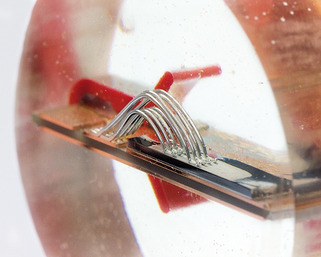
  • Consultancy on the different investigated failure modes, for instance chip damage due to improper bond wire process parameters
  • Partial discharge measurement
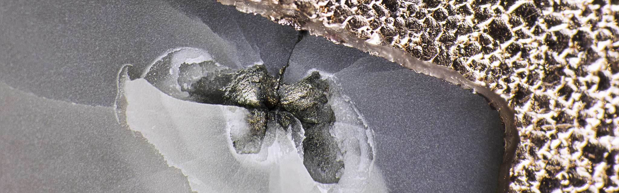
  • Optical microscopy for searching for dendrites
  • Laser interferometry (for analysis of coating quality and coating thickness)
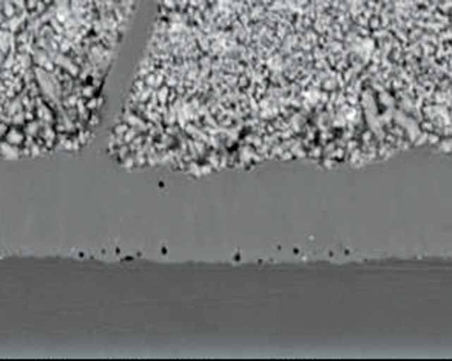
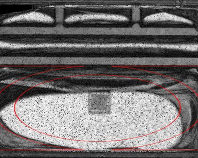
  • Cross-sectioning by sawing, grinding, polishing
  • Cross-sectioning by femto-laser curing
  • Comparative tracking index
  • Scratch test
  • Decapsulation of mold compounds as well as silicone gels
  • Scanning electron microscopy (SEM) and elemental analysis with energy dispersive X-ray spectroscopy (EDX), distribution and quantity
  • Focused ion beam (FIB), high speed cutting by plasma
  • Thermogravimetric analysis (TGA) and differential scanning calorimetry (DSC)
  • Fourier-transform infrared spectroscopy (FTIR)
  • Radiography / computer tomography

Destructive and non-destructive analysis for power electronics

The analysis of different system components before and after targeted aging as well as from field returns can be performed using imaging procedures and other characterization methods.

To expose system components, devices or modules can be decapsulated. Various etching processes and laser ablation are available for this purpose.

Destructive analysis

Demolded IGBT and diode of an D2Pak device

© Fraunhofer IISB
Cross section of IGBT power module
  • Cross-sectioning
  • Optical microscopy (magnification up to 5000x)
  • Scanning electron microscopy (SEM)
  • Element analysis (EDX, distribution and quantity)
  • Focused ion beam (FIB)
  • Decapsulation of mold compounds and silicone gels
  • Chemical removal of chip topside metallization and contacts, for instance bond wires and ribbons out of different materials
  • Nanoindentation, tensile tests under extended temperatures
  • Shear, pull and peel tests

Non-Destructive analysis

Focused ion beam analysis of an IGBT

  • Scanning acoustic microscopy (investigation of voids, cracks, delamination)
  • Partial discharge measurement for isolation quality investigations
  • Ultra-violet imaging of discharge effects
  • Infrared imaging, thermography for thermal resistance measurements
  • Lock-In-Thermography for localizing of defects
  • Eigen frequency measurement to determine cracks inside the material
  • Static and dynamic electrical characterization
© Fraunhofer IISB
Focused ion beam analysis of an IGBT
© Fraunhofer IISB
Scanning electron microscopy
© Fraunhofer IISB
Scanning acoustic microscopy of an DBC substrate with conchoidal fracture
© Anja Grabinger / Fraunhofer IISB

„Physics of Failure“ method

The „physics of failure“ method assists to get a better understanding of the reasons behind the symptom. Fraunhofer IISB helps to ask the right questions for the interpretation of failure analysis.


Failure-Mode: What kind of failure effect? Short/ open circuit, heating, etc

Failure-Cause: What kind of process? Crack formation and growth, migration, corrosion, etc

Failure-Mechanism: What triggers the failure? Bond wires, solder layer, cooling, etc.

Failure-Model: How can the failure be described? Mathematical or statistical model, FEM simulation, etc.