 Fraunhofer Institute for Integrated Systems and Device Technology IISB
Inorganic thin films for large-area coating and printing are provided for functional electrodes and electronic applications. Besides facile and low-cost processing, low temperature drying and conversion is a major research goal, making the films applicable to a wide range of substrates.
Thin-Film Technologies
Examples

Printed TFT Gate Electrodes
Printed Electronics
Printing of electronic materials opens up a range of novel low-cost, low complexity,and large-area components, circuits, and systems on alternative (e.g. flexible) substrates. Fully or partially printed devices include antennas for RFID, thick-film sensors, or displays.
IISB research in printed electronics is focused on inorganic materials from synthesis through to system integration.
A joint working group with the Chair of Electron Devices at University of Erlangen (FAU) covers basic and applied research topics.

SEM Image of cubic CuO Particles, Inset: CuO-ink
Synthesis and Formulation
Functional nano materials for printed electronics are synthesized by gas-phase or wet chemical chemistry.
Composition, size, and morphology of particles and/or layers can be widely modified with regard to processing (e.g. melting point) or electrical (e.g.bad gap) behavior.
Synthesis of doped semiconductor nanoparticles, ternary, or quaternary metal oxide systems is a promising research arena. Ink properties like viscosity, surface energy, and vapor pressures can be tailored with respect to subsequent processing. Thus, functional features can be produced by various techniques including ink jet printing, spray pyrolysis, and screen printing.

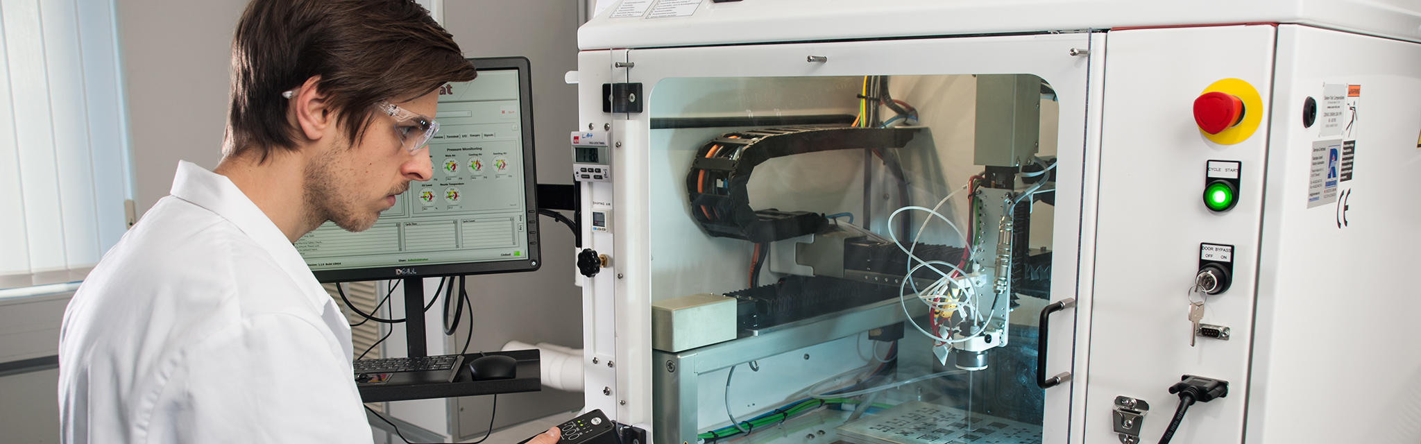
Inkjet Printer for Materials
Deposition and Ink Development
Structure Formation
Inks and precursor solutions are processed into thin films and structures by spin-casting or various printing methods. Substrates, inks, and processing conditions have to be carefully adjusted to give best results with respect to critical dimensions and electrical performance of the devices.
The formation of highly ordered layers and interfaces is not only important for the electrical behavior ofthe layers but also for the ability to stack several layers on top of each other. Also thermal and chemical compatibility of subsequently deposited materials have to be taken into account.

Low Temperature processed Thin Film Transistors based on Zinc Oxide
Low Temperature Thin-Film Technologies
Sensitive substrates like technical glasses or plastics for display or lighting applications demand for low temperature deposition techniques. Aiming at system integration Fraunhofer IISB offers deposition services as well as R&D know-how for the improvement of thin-films and devices.
The team has long-term expertise in process and equipment development for physical (PVD) and chemical vapor deposition (CVD), the latter ranging from conventional low-pressure CVD through metal organic CVD to plasma-enhanced or atomic-layer deposition techniques. Recent projects include sputtering of metal oxides for use in thin-film transistors.

Silicon Wafer with Thermoelectric Generators based on doped Poly Silicon
Silicon Process Integration
Based on a range of lithographic techniques like proximity printing (mask aligner), laser, and e-beam writing and accompanying etching techniques, Fraunhofer IISB offers various opportunities for the development of application-specific micro- and nanoelectronics, -fluidics, and –mechanics applications. In addition to photolithographic structuring, several elaborated resist systems are further utilized for sealing of surfaces and temporary or permanent joining of wafers.