Operando and in-line Analytics

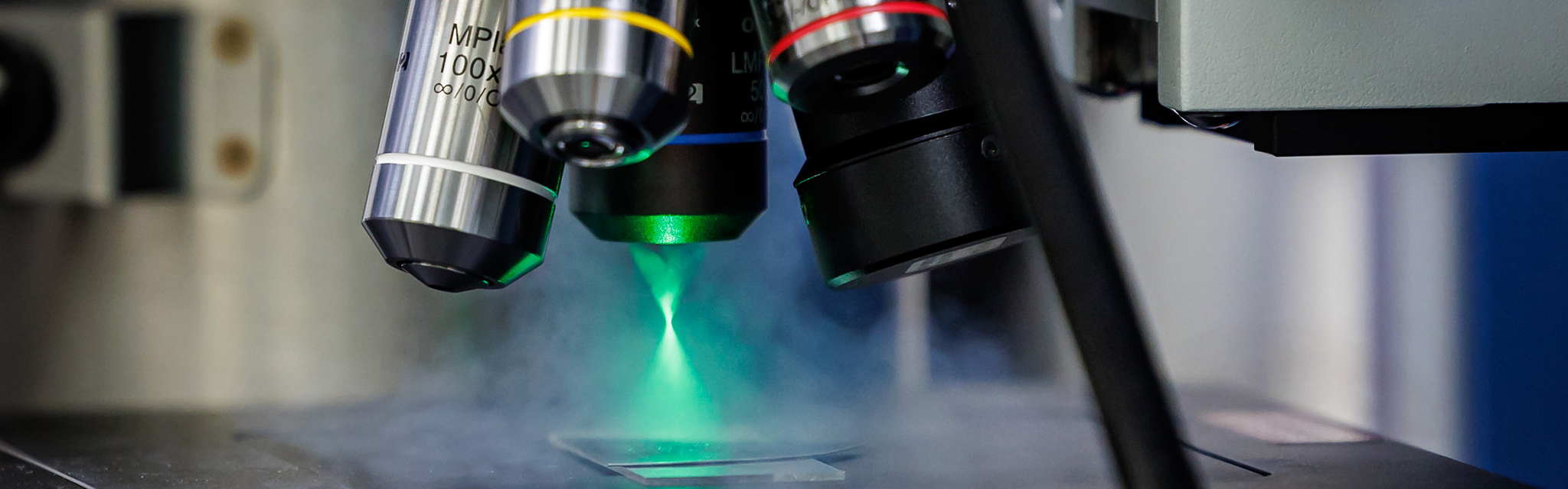
In recent years, the demands on the flexibility and functionality of semiconductor base materials for applications in power and communication electronics have grown enormously. Compound semiconductors play a particularly important role in this area. These materials have physical properties for such applications that are superior to those of the established silicon. In addition, defects in these materials are candidates for the realization of isolated quantum states for future highly sensitive quantum sensors or ultra-powerful quantum computers.

We have in-depth expertise in characterizing the optical, structural, physical and chemical properties of different crystal and wafer materials. This enables us to carry out service measurements for our customers within a short return time. The subject of our research is operando characterization, i.e. the investigation of (test) devices in operation. Such measurements make it possible to test the performance and reliability of devices. With a comprehensive defect analysis at an early stage of material development, critical defects for the reliability of the devices can be identified. Together with our customers, we find solutions to avoid these critical defects.

Optical Semiconductor Characterization

Application-oriented material characterization and defect analysis of semiconductor materials, crystals and epitaxial layers

As part of our research and services, we carry out the material characterization of semiconductor materials, crystals and epitaxial layers using optical defect spectroscopy.  

Key topics:

  • Micro-Raman spectroscopy
  • Photoluminescence spectroscopy (PL)

Services:

  • PL imaging for qualitative mapping of lateral inhomogeneities of charge carriers or their interaction with extended defects (spatial resolution ≥2 µm, sample size ≤180 × 180 mm2)
  • Confocal micro-Raman spectroscopy for monitoring residual mechanical stresses and charge carrier concentrations (spatial resolution ≥1 µm, sample size ≤100 × 100 mm2)
  • Measurement of lateral photovoltage (LPS) to determine phase boundaries, for example in Cz-Si (sample size ≤280 × 280 mm2)
  • FTIR spectroscopy, for example to detect the concentrations of oxygen, carbon and nitrogen dissolved in the silicon lattice (spatial resolution ≥15 µm, sample size ≤90 × 70 mm2)
  • Development of customized measurement methods together with industrial partners in the field of metrology
© Daniel Karmann / Fraunhofer IISB
Characterization at low temperatures
© Daniel Karmann / Fraunhofer IISB
Measurement of laser power with the microscope

Structural Semiconductor Characterization

Examination of microstructural defects using high-resolution X-ray analysis

As part of our research and services, we carry out the structural characterization of crystals, substrates, epitaxial layers and thin-film systems.

Key topics:

  • Structural analysis with high-resolution X-ray diffraction (HRXRD) and X-ray reflectometry (XRR)
  • Qualitative and quantitative phase analysis using PXRD and Rietveld analysis
  • Microscopy: light microscopy (VIS, NIR), confocal laser scanning microscopy, scanning electron microscopy (SEM)

Services:

  • Phase and element analysis
  • Determination of grid parameters and residual stresses
  • Development of customized measuring methods together with measuring device manufacturers
© Daniel Karmann / Fraunhofer IISB
Transmission diffractometer for powder diffraction
© Daniel Karmann / Fraunhofer IISB
High-resolution 5-axis X-ray diffractometer SmartLab XE

Operando and in-line Analytics

Development of operando investigations on electronic (test) devices and in-line analysis of recycling processes

As part of our research, we carry out operando investigations on electronic (test) devices and in-line analysis of recycling processes. We use optical imaging, spectroscopic and X-ray methods.

Key topics:

  • Operando investigations on electronic modules
  • Imaging (spectroscopic) process monitoring of recycling processes
  • Usage and (further) development of AI-based evaluation algorithms

Services:

  • Development and implementation of operando and in-line measurement techniques
  • Thermochemical simulation for process analysis
© Daniel Karmann / Fraunhofer IISB
Cooling and heating chamber (77 K - 600 K) for semiconductor samples
© Daniel Karmann / Fraunhofer IISB
Positioning and adjustment on the goniometer table

Publications

Flyers & Brochures