 Fraunhofer Institute for Integrated Systems and Device Technology IISB
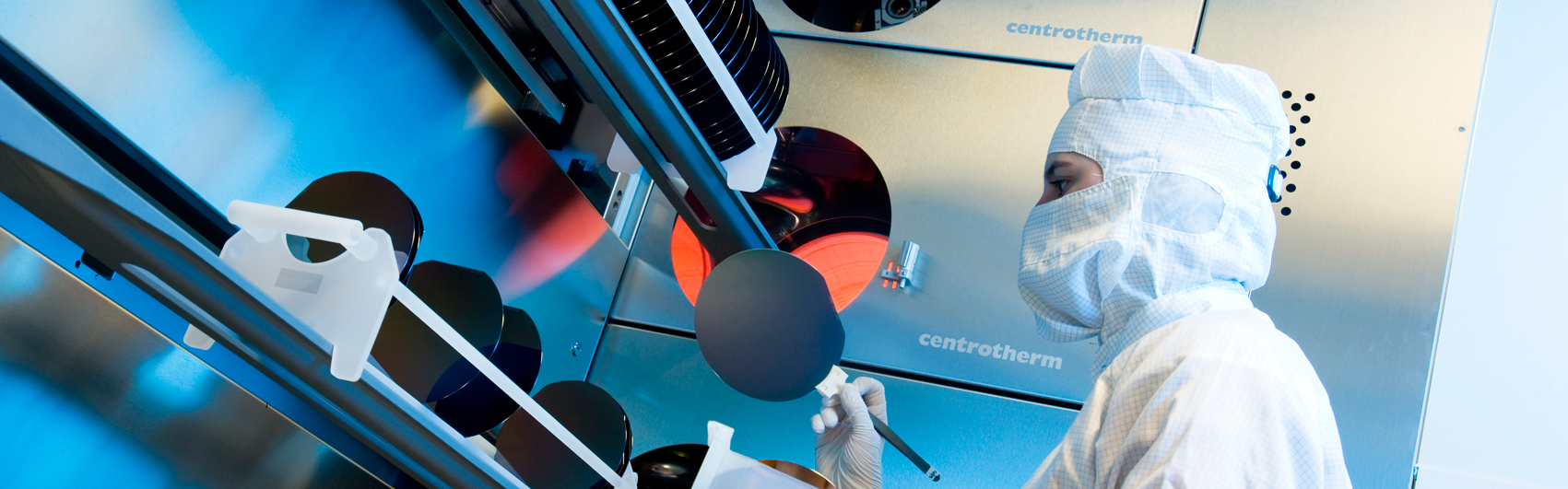
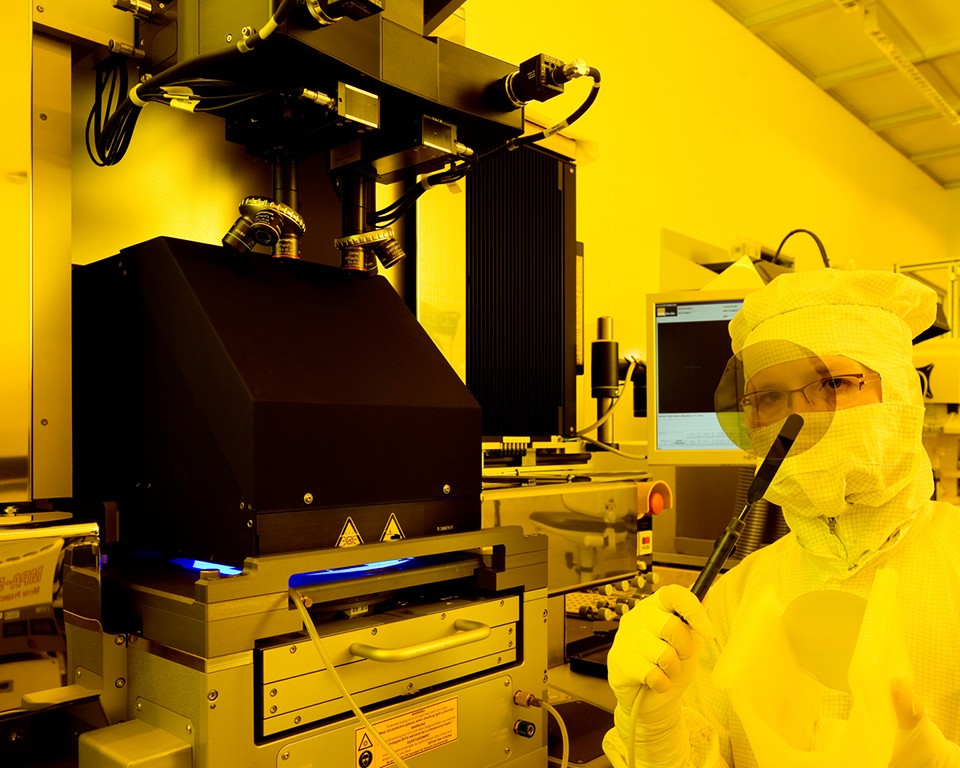
As part of the Research Fab Microelectronic Germany (FMD) we operate a continuous 150mm silicon carbide process line in an industry-compatible environment at our headquarter in Erlangen. With three decades of experience in microelectronics research and development we extended our activities to industry-oriented low-volume prototype fabrication of custom-tailored SiC devices, with a focus on power devices, CMOS devices, passives, sensors. Furthermore, we utilize a customized design of test devices, which are processed in our flexible fully CMOS equipped clean room facility in our subsidiary in Freiberg, in order to correlate the material properties to device performance and to identify device critical defects.
© Kurt Fuchs / Fraunhofer IISB
Test Devices
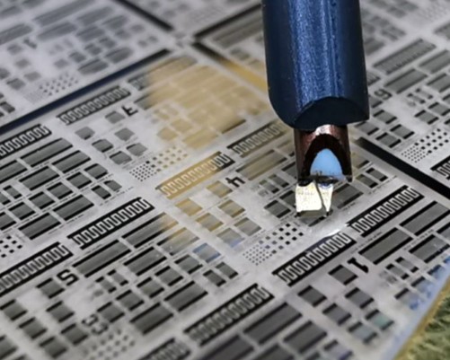
Optical inspection of a SiC wafer
AlN SAW structures on sapphire
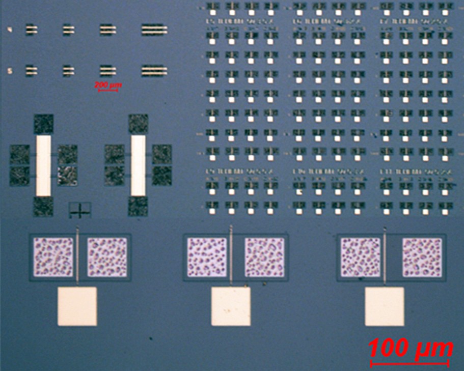
Microscopy image of GaN high-electron-mobility Transistors (HEMT) with varying gate length and other device test structures
Services
- Low-volume prototype fabrication of SiC devices
(e.g., JBS, VDMOS, diodes, CMOS) - Customized design of test devices
- Processing of test devices (e.g., GaAs, InP, GaN, AlN, AlScN, Diamond) in a flexible R&D line
- Development of device process steps (ALD, ALE, passivation, etching, metallization)
- Epitaxy (SiC, AlGaN)
- Identification of device critical materials defects
- Electrical characterization of devices on wafer level by IV, CV measurements